PCBA Manufacturing Process: The Professional Assembly Guide
The PCBA manufacturing process is a sophisticated journey that transforms a bare printed circuit board into a fully functional electronic assembly. Whether you are developing a complex industrial controller or a simple consumer gadget, understanding the nuances of assembly is crucial for ensuring product reliability and performance.
As a professional PCB and PCBA manufacturer with over 10 years of experience, WELLSPCBA has witnessed firsthand how a robust and meticulously tested assembly process can determine the success or failure of an electronic product launch.
In this guide, we will break down the professional manufacturing steps used by industry leaders like WellsPCBA to deliver high-quality electronic solutions. If you are new to this field, you might want to first understand what is PCBA manufacturing and how it differs from bare PCB fabrication in our PCB vs PCBA comparison.
Phase 1: Pre-Assembly Essentials
Before the first component is placed, several critical preparation steps must occur to prevent costly errors during mass production.
Design for Manufacturing (DFM) Check
A professional PCBA manufacturer always begins with a DFM check. This involves analyzing your PCB design files (Gerber files) to identify potential issues such as insufficient clearance, component spacing, or traces that might lead to soldering defects.
Components & PCB Sourcing
High-quality assembly starts with high-quality parts. This phase involves sourcing the bare PCBs and all electronic components (ICs, resistors, capacitors) according to the Bill of Materials (BOM).
Phase 2: The Core PCBA Manufacturing Steps
Modern electronics primarily rely on Surface Mount Technology (SMT), though Through-Hole Technology (THT) is still used for specific robust applications.
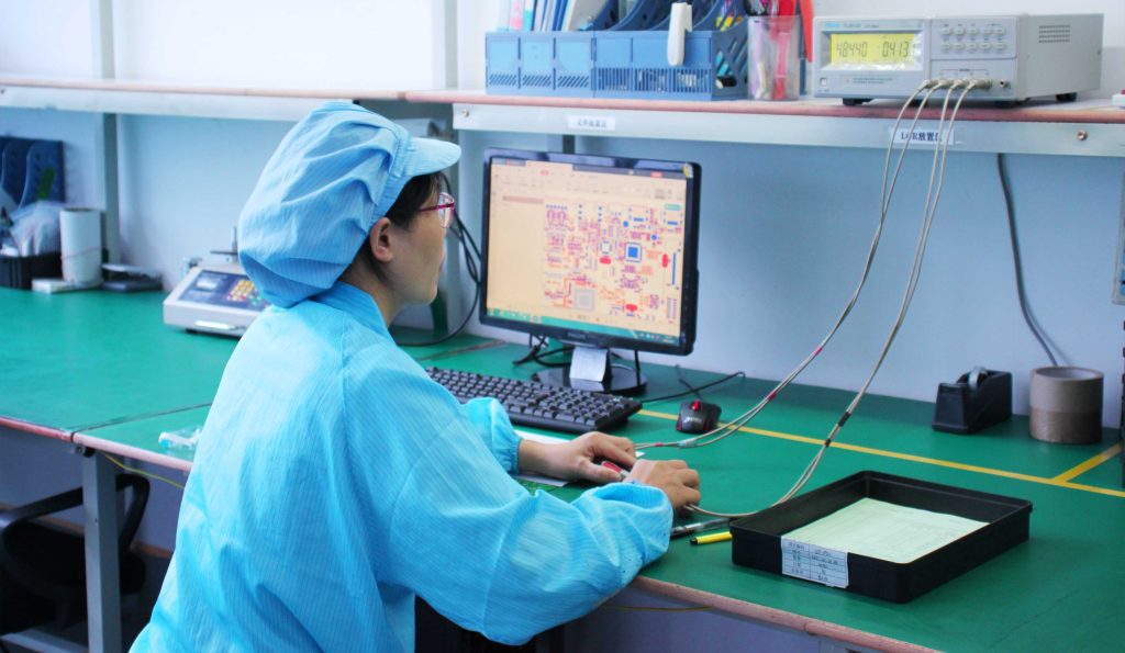
Step 1: Incoming Quality Control (IQC)
After receiving the components, a thorough Incoming Quality Control (IQC) is carried out. This includes verifying part numbers, quantities, and component conditions to rule out any defects. Moreover, implementing Electrostatic Discharge (ESD) protocols is vital to protect sensitive integrated circuits and other components during handling.
Step 2: PCB Cleaning
Before solder paste application, it’s crucial to clean the PCB using appropriate cleaning agents. This step removes oils, dust, and residues that may affect the adhesion of solder paste and the reliability of solder joints during reflow soldering.
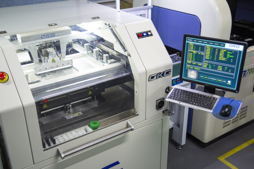
Step 3: PCB Stencil Making
A precision-designed stencil ensures uniform and accurate application of solder paste. Stencil apertures must align exactly with SMT pads, and any defect in stencil fabrication can compromise the entire SMT assembly.
Step 4: Solder Paste Stenciling
Solder paste application is a cornerstone of surface mount technology (SMT). The quality of solder paste printing directly impacts soldering effectiveness. The paste should be applied uniformly with the right squeegee pressure, and its management is critical to maintaining quality:
- The paste must be consumed within 24 hours of opening to maintain its effectiveness.
- The paste must be refrigerated between 0-10°C when not in use.
- The container should always be sealed tightly.
- Avoid leaving paste on the stencil for over 30 minutes to prevent degradation.
- Before use, it must be brought to room temperature for at least 2 hours and stirred for 3-5 minutes in the same direction using a tool with rounded edges to avoid damaging the solder balls.
- The paste must be consumed within 24 hours of opening to maintain its effectiveness.
Step 5: Pick and Place (PnP)
Next, the board moves to the Pick and Place machine. This high-speed robotic system “picks” surface mount components (SMDs) from reels and “places” them onto the solder paste with incredible precision.
Step 6: Reflow Soldering
Once the components are set, the PCB travels through a reflow oven. The oven applies controlled heat, melting the solder paste and creating permanent, solid electrical joints as the board cools.
Step 7: Through-Hole Component Insertion
For components like large connectors or electrolytic capacitors that require extra mechanical strength, Through-Hole Technology is used. These components are inserted into pre-drilled holes in the PCB.
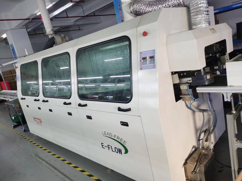
Step 8: Wave Soldering
For THT components, the board passes over a “wave” of molten solder. The solder wicks into the holes, securing the component leads to the board.Reflow soldering is at the heart of SMT (Surface Mount Technology). A properly defined temperature profile is essential to ensure consistent solder joints while preventing defects caused by overheating or insufficient cooling.
Inside a reflow oven, the temperature profile is typically divided into four key zones: Preheat, Soak (Thermal Soak), Reflow, and Cooling. Each stage has specific thermal requirements to ensure solder joint quality and component reliability.
1. Preheat Zone
The PCB is gradually heated to evaporate solvents and activate the flux.
As the PCB enters the preheat zone, solvents and volatile substances in the solder paste begin to evaporate. At the same time, the flux is activated, improving wetting on pads, component leads, and terminations. The solder paste softens and spreads, covering the pads and helping to prevent oxidation.
2. Soak Zone (Thermal Soak)
The temperature is stabilized to ensure uniform heating and minimize thermal shock.
In this stage, the PCB is evenly heated to allow all components to reach a consistent temperature. This prevents sudden temperature spikes when entering the reflow zone, reducing the risk of damage to both the PCB and sensitive electronic components.
3. Reflow Zone
The solder paste melts to form strong and reliable solder joints.
As the PCB reaches the reflow zone, the temperature rises rapidly above the solder’s melting point. The solder becomes liquid, wets the pads and component leads, and forms metallurgical bonds. Proper control in this phase ensures strong, defect-free solder joints.
4. Cooling Zone
Controlled cooling solidifies the solder and prevents defects such as cracking.
Finally, the PCB enters the cooling zone, where the solder solidifies to form stable joints. Controlled cooling is critical to avoid issues like thermal stress, cracking, or weak solder connections.
Maintaining an optimal solder joint profile throughout these stages is essential for achieving reliable connections and preserving the overall integrity of the PCB.
Phase 3: Post-Assembly & Quality Control
The manufacturing process isn’t complete without rigorous verification to ensure every connection is perfect.
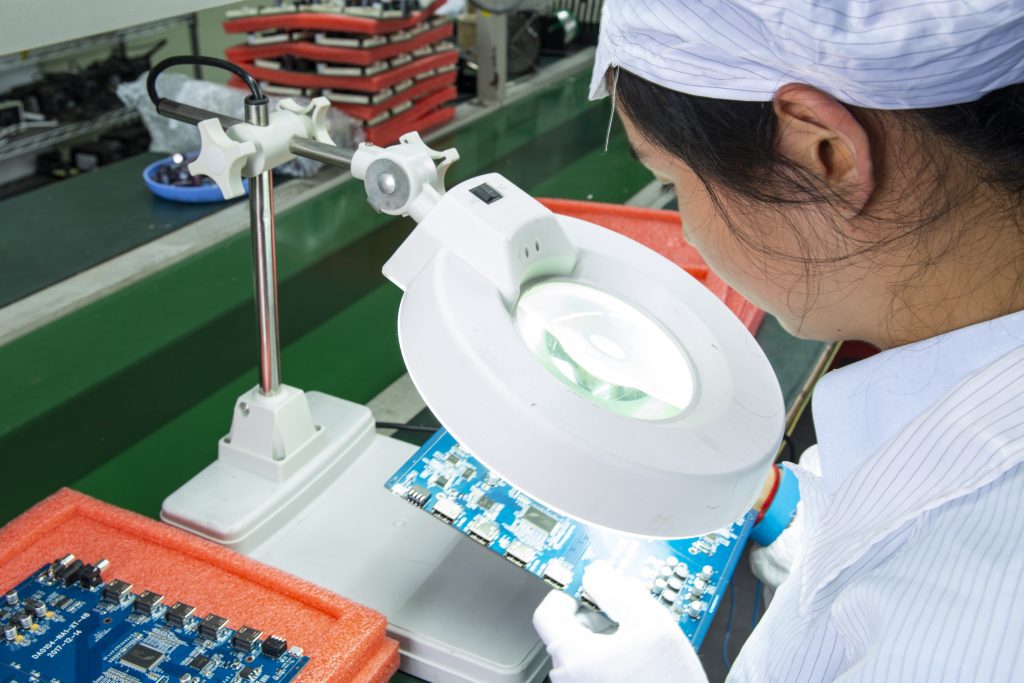
Automated Optical Inspection (AOI)
An AOI machine uses high-resolution cameras to scan the board for defects such as misplaced components, solder bridges, or dry joints. It is much faster and more accurate than manual inspection.
Both manual inspection and Automated Optical Inspection (AOI) systems are used to ensure solder joint quality and detect potential defects such as the following:
Cold Solder Joints (False/Weak Connections)
These joints may appear acceptable visually but fail to properly bond with the component leads or PCB pads. This defect is often caused by insufficient solder melting or poor wetting during reflow. As a result, the component may not form a reliable electrical connection, leading to functional failure.
Solder Bridging
Excess solder forms unintended connections between adjacent component leads, causing short circuits.
Dry Joints / Insufficient Soldering
These joints are mechanically weak and electrically unreliable, typically due to inadequate temperature or insufficient dwell time during soldering, resulting in poor contact.
Component Misalignment
Components may shift from their intended positions during the soldering process, leading to inaccurate placement and potential performance issues.
Solder Balls
Small spheres of solder may form during the reflow process. These can create a risk of short circuits if they come into contact with conductive areas.
Missing or Incorrect Components
Some components may be missing, improperly installed, or replaced with incorrect parts, leading to functional or reliability issues.
Poor Solder Joints
Solder joints may be too large, too small, or irregular in shape, which can negatively impact both electrical performance and mechanical strength.
Irregular Solder Shape
When solder joints deviate from their intended geometry, conductivity and structural integrity may be compromised. This issue is often caused by inconsistent solder paste application or improper soldering techniques.
By combining AOI systems with manual inspection, manufacturers can significantly improve defect detection rates and ensure higher reliability in PCB assembly.
X-Ray Inspection for BGA Components
For components like BGAs (Ball Grid Arrays) where the solder joints are hidden underneath the chip, X-ray inspection is mandatory to “see” through the package and verify the integrity of the hidden connections. integrity of the connections according to IPC Standards.
In-Circuit Testing (ICT) & Functional Testing (FCT)
Finally, the boards undergo electrical testing. ICT checks for shorts and opens, while Functional Testing powers up the board to ensure it performs its intended tasks correctly.
Phase 4: Final Touch & Cleaning
Flux Removal and Cleaning
Residual flux from the soldering process can cause corrosion over time. Professional manufacturers use deionized water or specialized cleaning agents to ensure the PCB is pristine.
Conformal Coating (Optional)
Depending on the application (e.g., aerospace or outdoor use), a thin layer of conformal coating may be applied to protect the PCBA from moisture, dust, and temperature extremes.
Final Quality Control (FQC)
Final Quality Control (FQC) involves a comprehensive end-of-line inspection. All inspection results are documented to ensure full traceability. This step guarantees that every PCBA meets both internal quality standards and customer-specific requirements.
Functional Testing (FT)
Functional Testing (FT) is performed on the printed circuit board assembly (PCBA) to verify that the final product operates as intended. This includes, but is not limited to, the following:
- Electrical Connectivity: Verifying electrical performance, including voltage, current, and power consumption.
- Communication Interfaces: Ensuring proper operation and reliability of interfaces such as UART, I²C, SPI, USB, HDMI, and Ethernet.
- Signal Integrity: Evaluating signal quality and timing accuracy.
- Memory Testing: Checking read/write functionality of RAM and flash memory.
- Functional Module Testing: Assessing the operation of components such as buttons, LED indicators, and sensors.
- Clock Testing: Verifying the frequency and stability of clock signals.
- Fault Detection and Tolerance Testing: Simulating fault conditions to evaluate the board’s fault tolerance capability.
- Software Testing: Validating the functionality and performance of embedded software or firmware.
Packaging
Finally, qualified products are packaged using appropriate protective materials to ensure safe transportation of the PCBA. Common protective packaging solutions include:
- Anti-static bags (ESD bags)
- Shock-absorbing foam or trays
- Moisture-proof packaging
- Wooden crates or frames for high-value goods
Packaging must be selected based on product fragility, transportation conditions, and customer specifications. Each packaging method has its own advantages and suitable applications. By choosing the right packaging solution, manufacturers can ensure that PCBA products are delivered safely and in perfect condition.
Common Challenges in PCBA Manufacturing
Even with automation, challenges such as Tombstoning (where a component stands up on one end) or Solder Bridging (accidental connection between two pads) can occur. Choosing an experienced partner like WellsPCBA ensures these risks are mitigated through advanced process control and expert engineering.
Conclusion
The PCBA manufacturing process is a delicate balance of precision machinery and expert oversight. By following these rigorous steps, manufacturers can ensure that every electronic device meeting the consumer’s hand is reliable and durable.
For a deeper look into the world of electronics, check out our PCBA Manufacturing Guide or learn more about the differences in PCB vs PCBA.