PCB Surface Finish Guide: HASL vs ENIG vs OSP vs ENEPIG — How to Choose the Right Option for Your Design
The PCB surface finish you specify on your fabrication drawing is one of the few decisions that simultaneously affects soldering yield, shelf life, high-frequency signal integrity, regulatory compliance, and unit cost. Engineers who treat it as an afterthought — accepting whatever the factory defaults to — routinely encounter tombstoning on fine-pitch passives, voided BGA joints, solder bridging on QFN pads, or assembly failures that trace back to a coating that degraded in the warehouse before the boards were ever reflowed.
This guide covers all six mainstream surface finish options with the technical depth that most manufacturer guides omit: exact plating thickness specifications, cost premium data, reflow cycle tolerance, and the high-frequency physics that makes nickel-bearing finishes unsuitable for RF designs above 1 GHz. Every recommendation in this guide corresponds to real production scenarios handled at Wells Electronics across 16+ years of PCB and PCBA manufacturing.
Quick Answer: HASL (lead-free) is the lowest-cost default for through-hole and coarse-pitch SMT. ENIG is the modern standard for fine-pitch SMT, BGA, and long shelf life. OSP is the cost-effective choice for high-volume single-pass SMT with short assembly windows. ENEPIG is the premium option when wire bonding or absolute black-pad elimination is required. Immersion Silver is the specialist choice for RF and high-frequency designs above 1 GHz. Immersion Tin is optimized for press-fit connector applications.
What You’ll Learn in This Guide
- The exact plating thickness, process chemistry, and failure mode of each of the 6 surface finish types
- Why ENIG’s black pad defect occurs, how to detect it, and what to demand from your supplier to prevent it
- The physics behind why nickel-bearing finishes (ENIG, ENEPIG) degrade signal integrity above 1 GHz
- Cost premium data referenced to LF-HASL baseline — the numbers no competitor guide publishes
- A 5-step selection framework you can apply to any design in under 10 minutes
- Industry-specific recommendations for medical, automotive, RF, consumer, and industrial applications
- What quality documents to request from your PCB manufacturer before confirming a surface finish order
What Is a PCB Surface Finish and Why Does It Matter?
The Function of a Surface Finish — Beyond Oxidation Prevention
A PCB surface finish is a protective coating applied to all exposed copper pads, vias, and lands on a finished circuit board. Without it, bare copper begins oxidizing within hours of air exposure — forming cupric oxide (CuO) and cuprous oxide (Cu₂O) layers that are non-solderable. A board with oxidized pads cannot form reliable intermetallic bonds during soldering, leading to cold joints, poor wetting, and outright assembly failures.
But oxidation prevention is only the first function. A surface finish performs three distinct roles throughout a board’s life:
Function 1 — Oxidation barrier during storage: Protects copper from the time of fabrication until the board reaches the assembly line, whether that is 10 days or 14 months later.
Function 2 — Solderability interface during assembly: Provides the metallurgical surface onto which solder paste wets, flows, and forms intermetallic compounds (IMCs) during reflow. The chemistry and topography of the finish directly determine solder joint quality.
Function 3 — Electrical contact surface in operation: For edge connectors, test points, and press-fit contacts, the finish remains the active electrical interface throughout the product’s field life. Durability, contact resistance, and wear resistance all depend on finish selection.
Choosing the wrong finish affects all three functions simultaneously. A finish that degrades during storage (OSP past its assembly window) prevents function 2 from ever occurring. A finish that produces surface roughness (HASL on a 0.4mm-pitch BGA) makes function 2 unreliable. Understanding the PCBA manufacturing process end-to-end helps clarify where surface finish decisions have the greatest production impact.
Two Categories: Metallic vs. Organic Finishes
Surface finishes fall into two fundamentally different protection mechanisms:
Metallic finishes (HASL, LF-HASL, ENIG, ENEPIG, Immersion Silver, Immersion Tin) deposit a metal or metal alloy layer over the copper. They protect through physical barrier — the deposited metal prevents oxygen and moisture from reaching the underlying copper. Metallic finishes are generally more durable, have longer shelf lives, and are more tolerant of handling and environmental variation.
Organic finishes (OSP — Organic Solderability Preservative) deposit a thin organic molecular film that bonds chemically to the copper surface through coordinate bonding. The film prevents oxidation as long as it remains intact. OSP is lower cost and produces the flattest possible surface, but the organic film is sensitive to heat, humidity, and repeated handling — it does not survive multiple reflow cycles intact.
This fundamental distinction drives the majority of surface finish selection decisions. If your application requires long shelf life, multiple reflow passes, or rework capability, an organic finish is not your option. If maximum flatness and minimum cost are the priorities for a well-controlled assembly operation, OSP is worth serious consideration.
The 6 PCB Surface Finish Types — Full Technical Breakdown
Surface finish selection should begin with technical specification, not with price. Understanding what each finish is made of, how it is deposited, and where it fails will always lead to a better decision than reading a bullet-point pros/cons list.
1. HASL — Hot Air Solder Leveling: The Traditional Workhorse
HASL is the original mass-production surface finish, dominant from the 1970s through the mid-2000s and still the default for many through-hole and mixed-technology designs. The process immerses the bare PCB in a bath of molten solder (traditionally Sn63/Pb37, or lead-free SAC305 alloy for the modern LF-HASL variant), then withdraws the board through a pair of hot air knives that remove excess solder with compressed air at approximately 260–270°C.
Exact technical parameters:
- Coating thickness: 1–40 µm (highly variable; this variability is the defining weakness)
- Solder alloy — traditional: Sn63/Pb37 (eutectic, melting point 183°C)
- Solder alloy — lead-free: SAC305 (Sn96.5/Ag3/Cu0.5, melting point 217–221°C)
- Process temperature: 255–270°C bath temperature
- Surface roughness: Ra 2–10 µm (significantly rougher than ENIG or OSP)
The thickness range of 1–40 µm is not a specification — it is an inherent characteristic of the hot-air leveling process. Solder accumulates more heavily on larger pads, inside via barrels, and at pad corners, while fine-pitch pad arrays between components receive thinner coverage. This means that on a board with mixed component types, different pads carry different solder volumes before any solder paste has been applied, making paste volume prediction unreliable.
Where HASL works well:
- Through-hole assemblies and mixed SMT/THT boards where the THT components dominate
- Designs with component pitch of 0.65mm or greater — at this pitch, the surface variation is within tolerable limits for reliable soldering
- Rapid prototypes where lead time and cost are the primary constraints
- Designs that will be assembled immediately — HASL shelf life exceeds 12 months under standard storage
Where HASL fails:
- Any board with BGA, CSP, or µBGA packages — the uneven pad heights across the BGA footprint prevent uniform solder joint formation
- Fine-pitch QFP or QFN with pitch below 0.5mm — the surface topography variation causes solder bridging between adjacent pads during reflow
- High-frequency designs — the rough surface and high-tin alloy contribute to signal scattering at microwave frequencies
- Export to EU, UK, or California markets — traditional Sn/Pb HASL violates RoHS regulations. LF-HASL is compliant but carries a small cost premium
For boards using through-hole technology extensively, understanding the full THT assembly process helps clarify why HASL’s superior barrel fill capability makes it the preferred finish for wave soldering applications.
2. ENIG — Electroless Nickel Immersion Gold: The Modern Standard
ENIG has become the default surface finish for modern SMT-dominated PCB designs, and for good reason. It provides the combination of properties — surface flatness, corrosion resistance, and shelf life — that BGA-dense, fine-pitch designs require. The process deposits two sequential layers: first, an electroless nickel layer via autocatalytic plating, then a thin immersion gold layer via displacement reaction.
Exact technical parameters (per IPC-4552B):
- Nickel layer: 3–5 µm (IPC-4552B minimum: 3 µm)
- Gold layer: 0.05–0.125 µm (this range is critical — too thick increases black pad risk)
- Surface roughness: Ra ≤ 0.8 µm
- Nickel phosphorus content: 7–11 wt% (this parameter directly controls black pad susceptibility)
- Shelf life: 12–18 months under standard storage conditions
The gold layer in ENIG serves only one purpose: protecting the nickel from oxidation during storage. During soldering, the thin gold layer dissolves into the solder within seconds of reflow, and the solder joint forms primarily against the nickel surface. This means the nickel layer is what actually determines long-term solder joint reliability — and nickel quality is what the black pad defect attacks.
Why ENIG dominates for BGA designs: The Ra ≤ 0.8 µm surface roughness creates a pad surface that is flat to within 0.1 µm variation across a BGA footprint, compared to HASL’s 2–10 µm variation. For a 0.8mm-pitch BGA with 200+ balls, this flatness uniformity is the difference between a 99.5% first-pass yield and a 94% yield that requires X-ray inspection and rework on every board. ENIG is also fully compatible with lead-free SAC alloy soldering and meets the RoHS Directive requirements for all major markets.
Where ENIG is the right choice:
- Any design with BGA, CSP, or flip-chip packages
- Fine-pitch QFP or QFN with pitch below 0.5mm
- Medical, automotive, and aerospace applications requiring IPC Class 3 workmanship
- Products with supply chain uncertainty — if boards may sit in inventory for 6–18 months before assembly, ENIG is the minimum viable shelf life for most supply chains
- Designs requiring multiple reflow passes or field rework — ENIG maintains solderability through three or more reflow cycles
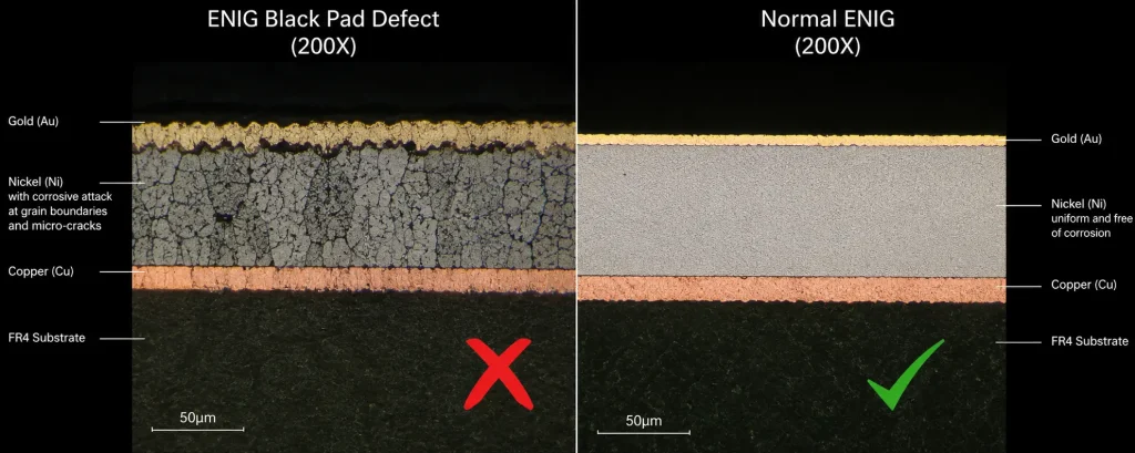
The Black Pad Problem: What It Is, Why It Happens, and How to Verify Your Supplier Controls It
Black pad is the most significant quality risk specific to ENIG — and the most poorly understood one. Nearly every competitor guide mentions it in a single sentence. It deserves a full explanation because, unlike most PCB defects, black pad cannot be detected before assembly.
What black pad is: During the ENIG gold deposition step, the displacement reaction between gold ions in solution and the underlying nickel is chemically aggressive. In a properly controlled bath, this reaction deposits gold uniformly while causing only minimal nickel surface dissolution. In a bath with low pH, high gold concentration, or excessive dwell time, the reaction becomes hyper-corrosive — attacking nickel grain boundaries, leaching phosphorus from the nickel structure, and leaving a corroded, phosphorus-enriched layer at the nickel surface. This corroded layer is brittle and has poor bond strength with the solder IMC. Under mechanical stress — press-fit insertion, connector mating, or thermal cycling — the solder joint fails catastrophically through the corroded nickel interface. When the fracture surface is exposed, it appears black or dark gray — the origin of the name.
What makes black pad insidious: A board with black pad defects looks completely normal. Visual inspection, AOI, and even X-ray inspection cannot detect the defect because the corroded nickel is hidden beneath an intact gold layer and a visually normal solder joint. Black pad only reveals itself under mechanical stress or thermal cycling — by which time the board may be in the customer’s product.
The three conditions that cause black pad:
- Gold bath pH below specification (typically should be controlled at 4.5–5.5)
- Nickel bath phosphorus content outside the 7–11 wt% range
- Gold layer thickness exceeding 0.15 µm, which corresponds to excessive dwell time in the gold bath
How to verify your supplier controls it:
Before placing an ENIG order, request the following documentation:
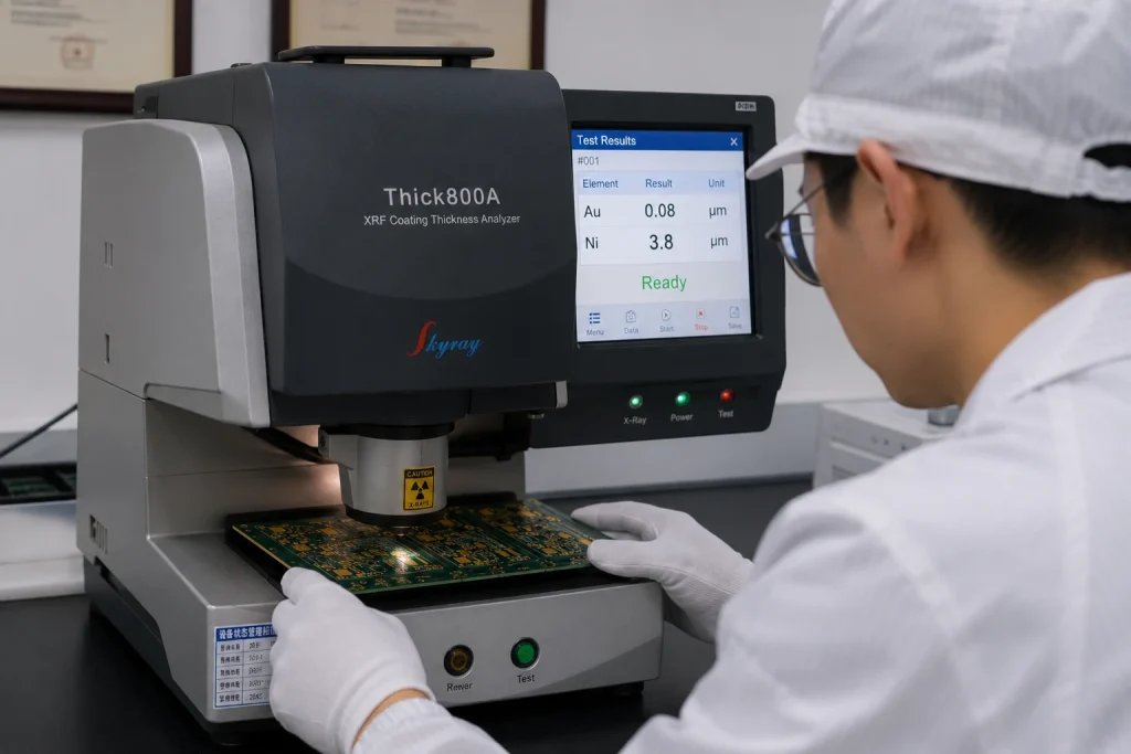
- IPC-4552B compliance declaration — confirms the factory operates to the current ENIG specification standard
- XRF thickness measurement report for the batch — shows gold layer thickness by pad location; gold should be uniformly within 0.05–0.125 µm; any measurement above 0.15 µm is a concern
- Nickel bath chemistry record — phosphorus content, stabilizer concentration, and bath age for the plating run that produced your boards
- Gold bath pH log — daily pH measurement records; variance outside 4.5–5.5 warrants explanation
At Wells Electronics, every ENIG order includes XRF thickness verification on production coupons, with gold and nickel thickness measurements documented in the shipment quality record. Nickel bath chemistry is monitored daily, with bath replenishment triggered by phosphorus content deviation rather than by calendar interval. ENIG boards that fail XRF specification are replated before shipment — not shipped with a deviation waiver.
If a supplier cannot provide an XRF thickness report on request, that is a significant quality flag. Consider upgrading to ENEPIG if your application cannot tolerate even low black pad risk.
3. ENEPIG — Electroless Nickel Electroless Palladium Immersion Gold: Premium Reliability
ENEPIG is ENIG with one additional layer inserted between the nickel and gold: an electroless palladium (Pd) layer. This seemingly minor addition has two major consequences that make ENEPIG the choice for the most demanding applications.
Exact technical parameters:
- Nickel layer: 3–5 µm (same as ENIG)
- Palladium layer: 0.05–0.15 µm (the critical addition)
- Gold layer: 0.03–0.05 µm (thinner than ENIG — palladium handles the protection role)
- Shelf life: 12 months or more
Why palladium eliminates black pad: The palladium layer acts as a physical diffusion barrier between the gold deposition bath and the nickel surface. It intercepts the aggressive gold displacement reaction before it reaches the nickel grain boundaries, preventing the hyper-corrosion that creates the phosphorus-enriched brittle zone. With ENEPIG, the gold layer dissolves into solder during reflow as it does with ENIG, but the palladium layer remains in the joint structure as a beneficial IMC constituent — it does not create a reliability problem.
Why ENEPIG enables wire bonding: ENIG’s gold layer, at 0.05–0.125 µm, is too thin to support thermosonic gold wire bonding or aluminum wire bonding. The gold-palladium surface in ENEPIG provides a bondable interface that ENIG cannot. For IC packages requiring wire bonding between die and substrate — flip-chip designs, MEMS sensors, multi-die modules — ENEPIG is the only standard surface finish option.
Where ENEPIG is the right choice:
- Any design requiring both soldering and wire bonding on the same substrate
- Aerospace, military, and implantable medical applications where black pad risk is unacceptable
- High-reliability automotive electronics (ISO 26262 ASIL C/D) where field failure analysis must not reveal plating quality as a contributing cause
- Mixed-technology boards combining THT, SMT, BGA, and press-fit connectors, all requiring one universal finish
The cost premium over ENIG (typically 80–150% above LF-HASL baseline versus ENIG’s 30–60%) is significant. For most industrial and commercial applications, properly controlled ENIG with XRF verification provides sufficient reliability. ENEPIG becomes necessary when the application consequence of a black pad failure is unacceptable — patient injury, flight-critical system failure, or irretrievable field deployment.
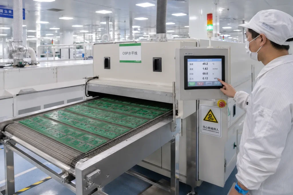
4. OSP — Organic Solderability Preservative: High-Volume SMT’s Optimal Choice
OSP is the outlier among PCB surface finishes. While all other finishes deposit a metallic or inorganic layer, OSP applies a thin organic molecular film — typically a benzimidazole-based compound — that bonds to the copper surface through coordination chemistry, forming a chelated copper complex. The film is transparent, extremely thin, and provides the flattest possible soldering surface.
Exact technical parameters:
- Coating thickness: 0.2–0.5 µm (so thin it is essentially invisible; this also means it cannot be measured by standard XRF)
- Chemical composition: Benzimidazole or substituted benzimidazole compound
- Shelf life: 6–12 months (strongly dependent on storage temperature and humidity)
- Maximum reflow cycles: 1–2 (organic film degrades significantly beyond the first reflow)
- Storage requirement: 15–25°C / RH ≤ 60%; boards should not be removed from sealed packaging until immediately before assembly
Why OSP excels in high-volume SMT production: The 0.2–0.5 µm OSP coating adds essentially zero height to the copper pad surface, making OSP the flattest of all surface finish options — even flatter than ENIG, which adds 3–5 µm of nickel plus gold. This near-zero surface addition makes OSP the optimal finish for high-volume PCB assembly lines running fine-pitch SMT with automated solder paste inspection (SPI). When every pad height is exactly copper level, paste volume prediction from the stencil aperture design is maximally accurate, and SPI rejects are minimized.
OSP is also the only RoHS-compliant surface finish that costs at or below LF-HASL pricing. For a consumer electronics product with 50,000-unit monthly volume, an OSP cost saving of $0.05–0.10 per board adds up to $2,500–5,000 per month — meaningful at scale.
Where OSP fails:
- Any board with through-hole components: OSP coating inside via barrels is non-uniform and thermally fragile; wave soldering through OSP-coated holes produces unreliable barrel fill
- Second-side reflow assemblies: boards going through reflow twice reach the second pass with significantly degraded OSP on the bottom side, risking poor wetting on bottom-side components
- Products with uncertain assembly timing: if boards will sit in your warehouse for more than 6–8 months, or if your assembly line schedule is uncertain, OSP’s shelf life becomes a real risk
- Boards requiring field rework: the OSP film cannot survive the localized heating of rework, making resoldering on reworked areas unreliable without a separate flux application step
5. Immersion Silver — The RF and High-Frequency Specialist
Immersion Silver (IAg) is a displacement-plated finish that deposits a thin silver layer directly onto the copper surface. Silver’s conductivity (6.30 × 10⁷ S/m) is slightly higher than copper’s (5.96 × 10⁷ S/m) and dramatically higher than nickel’s (1.43 × 10⁷ S/m). This electrical property makes Immersion Silver the specialist choice for RF and high-frequency circuit designs — for reasons that go deeper than conductivity alone.
Exact technical parameters:
- Silver layer thickness: 0.12–0.4 µm
- Shelf life: 6–12 months (sensitive to sulfur-containing environments)
- Surface resistivity: lowest of all common finishes (matched to or slightly better than copper)
- Maximum reflow cycles: 1–2
The physics of why ENIG fails RF designs above 1 GHz — and why Immersion Silver does not:
At high frequencies, electrical current does not flow uniformly through a conductor’s cross-section. Instead, it concentrates increasingly toward the surface as frequency rises — a phenomenon called the skin effect. The skin depth (δ) in a conductor is given by δ = √(2ρ/ωµ), where ρ is resistivity, ω is angular frequency, and µ is magnetic permeability.
Nickel — the structural layer in both ENIG and ENEPIG — has a relative magnetic permeability (µr) of approximately 1.8 to 10, depending on phosphorus content and microstructure. This means nickel is a ferromagnetic material. At 1 GHz, the skin depth in nickel is approximately 0.5 µm. At 10 GHz, it falls below 0.2 µm.
The consequence: at microwave frequencies, the electromagnetic field penetrates the ENIG surface, encounters the nickel layer (which begins 0.05–0.125 µm below the gold surface), and induces current flow through a ferromagnetic material with both higher resistivity and higher permeability than copper. The result is elevated insertion loss — typically 0.3–0.5 dB/inch at 10 GHz compared to a copper or silver reference — that becomes significant in RF front-ends, antenna feed networks, filter circuits, and high-speed differential pairs.
Immersion Silver eliminates the ferromagnetic nickel layer entirely. Signal current at GHz frequencies flows through the silver film directly into the copper below, encountering no magnetic material in its path. For antenna boards, phased array substrates, 5G millimeter-wave modules, and PCIe Gen 5 or 112G SerDes designs where signal integrity margins are tight, Immersion Silver is the technically correct surface finish choice.
The main risks of Immersion Silver:
Creep corrosion is the primary reliability concern. Silver reacts with atmospheric sulfur compounds (H₂S, SO₂) to form silver sulfide (Ag₂S), a non-conductive black corrosion product. Unlike bulk corrosion, silver sulfide can migrate laterally across the pad surface and between adjacent conductors under humid conditions — “creeping” across distances that can eventually bridge pads. Industrial environments with elevated sulfur content — near rubber processing, paper mills, or high-pollution areas — present elevated creep corrosion risk. Proper sealed packaging (anti-tarnish barrier bags with desiccant) and assembly within the shelf life window mitigate this risk.
Handling sensitivity is also significant. Fingerprint oils contain organic acids that visibly tarnish silver surfaces. All boards with Immersion Silver finish must be handled with powder-free gloves from the moment the package is opened.
6. Immersion Tin — The Press-Fit Connector Specialist
Immersion Tin (ISn) deposits a thin tin layer over copper through a displacement reaction, producing a flat, solderable surface that is particularly well-suited to press-fit connector applications. It is less commonly specified than ENIG or OSP but fills a specific technical niche.
Exact technical parameters:
- Tin layer thickness: 0.8–1.2 µm (IPC minimum: 0.8 µm)
- Shelf life: 3–6 months (the shortest of all standard surface finishes)
- Copper-tin intermetallic growth: begins immediately after deposition; accelerates above 40°C
Why Immersion Tin suits press-fit applications: Press-fit connectors are inserted by mechanical force into plated through-holes, relying on controlled elastic deformation between the connector tail and the hole wall to create a gas-tight electrical connection. The thin, compliant tin layer on the hole wall reduces insertion force while maintaining good contact resistance — properties that solder or hard gold finishes cannot provide at equivalent thickness.
The tin whisker problem: Tin is subject to spontaneous whisker growth — thin metallic filaments that can emerge from the tin surface over months to years under stress, temperature gradients, or electrical fields. Tin whiskers ranging from 0.1 to over 10 mm have been documented in electronic assemblies, and they are electrically conductive — capable of bridging adjacent conductors and creating shorts. Mitigation approaches include nickel underlayer (which reduces whisker driving force), controlled tin thickness, and avoiding high-stress storage conditions.
Where Immersion Tin is the right choice:
- Backplane and motherboard designs using press-fit connectors
- Designs requiring a lead-free, flat finish at lower cost than ENIG where the assembly window can be controlled to 3–6 months
- Applications where the tin whisker risk is acceptable given the design geometry (large pad pitch reduces bridging risk)
The Master Comparison Table
PCB Surface Finish — All 6 Types Side-by-Side
| Parameter | LF-HASL | ENIG | ENEPIG | OSP | Immersion Silver | Immersion Tin |
| Coating thickness | 1–40 µm | Ni 3–5 µm / Au 0.05–0.125 µm | Ni 3–5 µm / Pd 0.05–0.15 µm / Au 0.03–0.05 µm | 0.2–0.5 µm | 0.12–0.4 µm | 0.8–1.2 µm |
| Surface flatness | Poor | Excellent | Excellent | Excellent | Excellent | Excellent |
| Shelf life | 12 months+ | 12–18 months | 12 months+ | 6–12 months | 6–12 months | 3–6 months |
| Max reflow cycles | 3+ | 3+ | 3+ | 1–2 | 2–3 | |
| RoHS compliant | ✅ | ✅ | ✅ | ✅ | ✅ | ✅ |
| BGA compatible | ❌ | ✅ | ✅ | ✅ | ✅ | ✅ |
| Wire bonding | ❌ | Limited | ✅ | ❌ | ❌ | ❌ |
| High-freq (>1 GHz) | Poor | Poor (Ni loss) | Poor (Ni loss) | Good | Best | Good |
| Cost vs. LF-HASL | Baseline | +30–60% | +80–150% | +0–5% | +15–25% | +10–20% |
| Primary risk | Rough surface | Black pad | High cost | Short shelf life | Creep corrosion | Tin whiskers |
| IPC-4552 standard | IPC-4552A | IPC-4552B | IPC-4556 | IPC-4552A | IPC-4553 | IPC-4554 |
Cost Reality Check — What Surface Finish Actually Adds to Your Board Price
Surface finish cost is one of the least transparently discussed topics in PCB procurement. Every competitor guide says “HASL is cheapest, ENEPIG is most expensive” without giving the numbers that let you make an actual budget decision.
Surface finish typically contributes 5–15% of total bare board cost, depending on board complexity, copper area, and order volume. The main cost drivers are: gold and palladium commodity prices (ENIG and ENEPIG), chemical bath management complexity (ENIG, ENEPIG, Immersion Silver, Immersion Tin), and process cycle time.
Typical cost premium versus LF-HASL baseline
(standard 4-layer board, 100 × 100 mm, 1 oz copper, prototype quantities):
| Surface Finish | Typical Premium Range | Primary Cost Driver |
|---|---|---|
| HASL (Sn/Pb) | −5% (lower in some markets) | Lead-tin alloy cost advantage |
| LF-HASL | Baseline (0%) | — |
| OSP | +0–5% | Simple process; marginal chemical cost |
| Immersion Tin | +10–20% | Chemical bath management; tin cost |
| Immersion Silver | +15–25% | Silver commodity price |
| ENIG | +30–60% | Gold price + chemical process control |
| ENEPIG | +80–150% | Palladium + gold + added process complexity |
Important caveats: at volume production (1,000+ boards), ENIG’s premium typically compresses to +20–35% because gold bath utilization improves and process amortization spreads. OSP’s marginal cost advantage over ENIG often disappears when first-pass assembly yield differences are factored in — OSP’s storage sensitivity and single-reflow limitation can generate rework costs that exceed the finish savings on any order where assembly conditions are not tightly controlled.
The practical takeaway: for most commercial designs, the cost difference between LF-HASL and ENIG is $0.50–2.00 per board at prototype quantities. This is rarely the deciding factor in a design with $15–50 of component content. Optimize for yield and reliability first; optimize for finish cost only when all other selection criteria are equal.
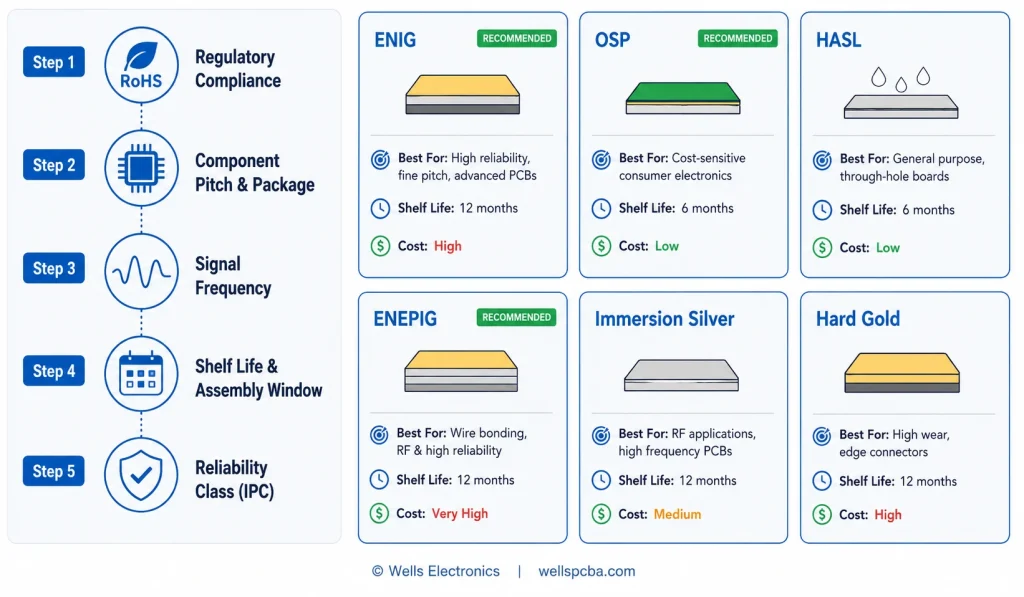
The 5-Step PCB Surface Finish Selection Framework
Apply these steps in sequence. Each step eliminates options; the remaining candidates at Step 5 are all viable, and the final choice is a cost and availability decision.
Step 1 — Confirm regulatory compliance requirements
Determine the markets your product will enter. Export to the European Union, United Kingdom, or California (under RoPHs-equivalent regulations) requires compliance with the RoHS Directive — which prohibits the use of lead (Pb) in electronic assemblies. Traditional Sn/Pb HASL is non-compliant and must be excluded. All other standard finishes (LF-HASL, ENIG, ENEPIG, OSP, Immersion Silver, Immersion Tin) are RoHS-compliant. Note that certain industrial equipment categories retain RoHS exemptions; confirm your product’s classification with your regulatory counsel before assuming compliance.
Step 2 — Evaluate minimum component pitch and package types
If your BOM contains any BGA, CSP, µBGA, or flip-chip package → eliminate HASL (both variants) immediately. If any component has a lead pitch below 0.5 mm (fine-pitch QFP, 0402 or smaller passives in dense arrays) → HASL is also eliminated. If the design includes wire bonding → only ENEPIG remains. For designs with all components at pitch ≥ 0.65 mm and no BGA → all finishes remain viable; continue to Step 3.
For guidance on how component pitch and package density interact with the DFM requirements for surface finish selection, see DFM in PCB Assembly.
Step 3 — Assess signal frequency requirements
If any signal net on the board operates above 1 GHz (RF front-ends, antenna feeds, mmWave interconnects, PCIe Gen 4/5 data lanes, 25G+ Ethernet lanes) → eliminate ENIG and ENEPIG due to the ferromagnetic nickel loss mechanism described in the Immersion Silver section above. The remaining options for high-frequency designs are: Immersion Silver (preferred), OSP (acceptable), and LF-HASL (marginal — the rough surface scatters high-frequency signals). If all signals operate below 1 GHz → all remaining options are electrically equivalent; continue to Step 4.
Step 4 — Determine shelf life and assembly window requirements
How long will boards sit between fabrication and assembly? If the answer is: under 30 days in a controlled environment → OSP is viable. Between 1 and 6 months → Immersion Silver, Immersion Tin, or ENIG. Between 6 and 18 months → ENIG is the standard choice; Immersion Silver is acceptable with proper sealed storage. Over 18 months, or genuinely uncertain → ENIG or ENEPIG only. Hard Gold for contact areas with wear requirements.
Step 5 — Match the reliability class of the application
Match to IPC-6012 performance class requirements. Class 1 (consumer, non-critical) → LF-HASL or OSP are sufficient. Class 2 (industrial, communications, computing) → ENIG is the standard; LF-HASL acceptable for coarse-pitch mixed-technology. Class 3 (high reliability: medical, automotive, military, aerospace) → ENIG with documented XRF verification, or ENEPIG. Class 3/A (space, life-critical implants) → ENEPIG or Hard Gold exclusively. (IPC-6012 standard)
Industry-Specific Surface Finish Recommendations
| Industry / Application | Recommended Finish | Key Reason |
|---|---|---|
| Medical devices (ISO 13485, IPC Class 3) | ENIG / ENEPIG | Long shelf life for regulated supply chains; full traceability; IPC Class 3 solder joint reliability |
| Automotive electronics (IATF 16949) | ENIG / ENEPIG | Wide-temperature solderability; multi-reflow tolerance; vibration-induced fatigue resistance at solder joints |
| Aerospace / Defense | ENEPIG / Hard Gold | Black pad unacceptable; maximum corrosion resistance; wire bonding capability |
| 5G / RF / Microwave (>1 GHz) | Immersion Silver / OSP | No ferromagnetic nickel; minimum insertion loss; surface uniformity for controlled impedance |
| Consumer electronics (high-volume SMT) | OSP / LF-HASL | Cost optimization; controlled assembly window; single-pass reflow |
| IoT hardware (medium-volume) | ENIG | Best overall cost-reliability balance; tolerates supply chain variability |
| Industrial control / VFDs | LF-HASL / ENIG | THT + SMT mixed assembly; cost-conscious with reliability baseline |
| High-speed digital (PCIe Gen 4/5, 112G) | Immersion Silver / ENIG | Signal integrity margin; ENIG acceptable below 15 GHz |
| Rapid prototyping | LF-HASL / OSP | Fastest turnaround; lowest incremental cost |
| Press-fit connector boards | Immersion Tin | Compliant tin layer for gas-tight press-fit joints |
What to Ask Your PCB Manufacturer Before Confirming Surface Finish
Most of the production problems that originate with surface finish selection are actually surface finish execution problems — the right finish specified, but applied by a supplier without adequate process controls. These are the questions and documents that separate a controlled process from a hope-based one.
Quality Documentation to Request
For ENIG and ENEPIG orders:
- IPC-4552B (ENIG) or IPC-4556 (ENEPIG) compliance declaration — confirms the factory operates to current specification
- XRF thickness measurement report for your production batch — gold layer must fall within 0.05–0.125 µm for ENIG; any measurement above 0.15 µm indicates process drift and elevated black pad risk
- Nickel bath chemistry record for the plating run — phosphorus content should be 7–11 wt%; deviation outside this range affects both solderability and corrosion resistance
- Gold bath pH log — should be maintained at 4.5–5.5; pH excursions below 4.5 are the primary driver of over-aggressive nickel attack
For further context on how these quality verification documents integrate with supplier qualification, see PCB coupon test station verification — coupon-based XRF measurement is the same methodology applied to surface finish verification.
For OSP orders:
- OSP chemical product technical datasheet — confirms maximum reflow temperature tolerance and rated shelf life under specified storage conditions
- Storage condition records for your boards — temperature and humidity logs for the period between fabrication and delivery
For Immersion Silver orders:
- Silver layer thickness measurement report — target 0.12–0.4 µm; thinner deposits are more susceptible to tarnishing
- Anti-tarnish packaging specification — confirms boards are packaged in sealed barrier bags with desiccant before shipment
For all finishes:
- IPC-6012 applicable class compliance declaration — confirms the fabrication process meets the workmanship standard for your specified class
Storage and Handling by Finish Type
| Finish | Storage Conditions | Maximum Window | Handling Notes |
|---|---|---|---|
| LF-HASL | Standard PCB storage | 12+ months | Normal handling |
| ENIG | Sealed packaging, standard conditions | 12–18 months | Normal handling |
| ENEPIG | Sealed packaging, standard conditions | 12+ months | Normal handling |
| OSP | 15–25°C, RH ≤ 60%; sealed | 6–12 months from fab | Do not open until assembly; assemble within 30 days of opening |
| Immersion Silver | Anti-tarnish barrier bag + desiccant | 6–12 months | Powder-free gloves required at all times; avoid sulfur-containing environments |
| Immersion Tin | Moisture barrier packaging | 3–6 months | Avoid mechanical contact; fragile thin coating |
How Wells Electronics Ensures Surface Finish Quality
At Wells Electronics, surface finish quality control is not a customer-requested add-on — it is a standard production requirement. For all ENIG orders, XRF thickness verification is performed on fabrication coupons from the production panel before any boards are released. Gold layer and nickel layer measurements are documented in the shipment quality record and available to customers on request.
ENIG chemical bath management follows daily monitoring protocols: nickel bath phosphorus content, stabilizer concentration, and gold bath pH are measured and logged every production day. Bath replenishment is triggered by parameter deviation, not by calendar interval. This approach prevents the gradual bath drift that produces black pad defects in factories that manage by time rather than by chemistry.
OSP boards are stored in a temperature and humidity controlled zone and managed under first-in, first-out (FIFO) inventory control, with the fabrication date marked on each package. Immersion Silver boards are packaged in anti-tarnish barrier bags with desiccant immediately after fabrication, with the assembly-by date printed on the outer label.
For designs requiring surface finish selection guidance before design is complete, Wells process engineers are available for pre-submission consultation at no charge. For a full picture of how surface finish specification fits into the broader design-to-delivery workflow, the Turnkey PCBA Guide covers every stage from Gerber file review through final shipment.
5 Surface Finish Mistakes Engineers Make — and How to Avoid Them
Mistake 1: Defaulting to HASL on a Fine-Pitch SMT Board
The scenario: a design with 0.4mm-pitch QFN, several 0402 passives, and a cost-conscious procurement team. HASL is specified because “it’s cheaper and we’ve always used it.” The result: inconsistent solder paste heights across QFN pads, bridging on 0402 arrays, and a first-article rework rate of 15–20%.
The fix: any board with component pitch below 0.5mm or any BGA/CSP package requires a flat finish. ENIG is the standard recommendation; OSP is acceptable if the assembly window is controlled. The HASL cost saving of $0.50–1.00 per board is erased by a single rework incident.
Mistake 2: Specifying OSP Without Defining the Assembly Window in the Purchase Order
OSP’s shelf life is quoted as 6–12 months, but this assumes the boards remain in sealed packaging and are stored under controlled conditions. Once the package is opened, the organic film begins degrading — and the first reflow accelerates that degradation significantly. A board opened, partially assembled, and reflowed again two weeks later may have OSP on its unassembled pads that is at the margin of solderability.
The fix: define the maximum time from package opening to first reflow in your purchase order or incoming inspection criteria. 30 days is a reasonable and conservative limit. If your assembly schedule cannot reliably meet this window, switch to ENIG.
Mistake 3: Specifying ENIG on an RF Board Without Checking Operating Frequency
The scenario: a 2.4 GHz Wi-Fi module designed with ENIG because “it’s the standard finish.” At 2.4 GHz, ENIG’s nickel loss contribution is moderate — perhaps 0.15–0.2 dB/inch above the copper baseline. For a short RF trace, this may be within margin. At 5 GHz, 24 GHz, or 77 GHz, the insertion loss penalty compounds and can push a marginal design below the link budget.
The fix: for any board with RF traces, antenna elements, or baluns above 1 GHz, model the insertion loss with the surface finish’s nickel layer included. If the margin is less than 3 dB, switch to Immersion Silver. The cost difference is marginal; the signal integrity improvement is real.
Mistake 4: Placing an ENIG Order Without Requesting an XRF Report
If black pad occurs in your production, root-cause analysis will eventually trace it to the gold plating bath chemistry at the time of fabrication. By that point, the bath records may no longer exist, and the factory will have no accountability mechanism. The only reliable protection is requesting XRF documentation at the time of order.
The fix: add a line to your standard ENIG purchase order: “XRF thickness report for gold layer (Au, all production coupons) required with shipment.” A supplier that refuses or cannot produce this report is not operating an adequately controlled ENIG process. See how to choose a PCBA manufacturing partner for more supplier qualification criteria.
Mistake 5: Changing Surface Finish Mid-Program Without Re-Running DFM
Surface finish selection affects not just the pad coating but the pad design itself. ENIG is typically applied to non-solder-mask-defined (NSMD) pads — where the solder mask opening is slightly larger than the copper pad — which is the recommended configuration for BGA and fine-pitch SMT. OSP is compatible with both NSMD and solder-mask-defined (SMD) pad configurations. HASL is often used with slightly different aperture ratios in the SMT stencil to account for the existing solder volume on the pad.
Switching from ENIG to OSP midway through production, or from HASL to ENIG when a design matures, requires a DFM re-review of pad geometry and stencil aperture specifications. Skipping this step introduces yield variation that engineering teams often attribute to assembly process variation when the root cause is a pad design mismatch with the new finish.
Frequently Asked Questions
ENIG is the standard choice for BGA packages at any pitch. Its Ra ≤ 0.8 µm surface flatness ensures uniform solder ball contact across the entire BGA footprint, which is the primary requirement for high assembly yield on fine-pitch BGAs. For pitch at or below 0.4 mm, or for BGAs on assemblies requiring simultaneous wire bonding, ENEPIG provides additional reliability margin — specifically eliminating black pad risk that, while low in a well-controlled ENIG process, is not zero. OSP is a technically viable alternative for BGA at moderate pitch in high-volume applications where the assembly window can be tightly controlled.
Yes, for the right designs. LF-HASL remains the optimal choice for through-hole assemblies and mixed SMT/THT boards where wave soldering dominates, for rapid prototypes requiring minimum cost and maximum fabrication speed, and for coarse-pitch designs (≥ 0.65 mm) where surface flatness is not a constraint. The estimated 70% global market share of HASL cited by several industry references reflects the large installed base of through-hole and coarse-pitch production still running worldwide. HASL is not obsolete — it is simply not appropriate for modern fine-pitch SMT or BGA assembly.
Black pad is a hyper-corrosion defect at the nickel-gold interface caused by an over-aggressive gold displacement reaction during ENIG plating. The gold bath attacks nickel grain boundaries, concentrating phosphorus in a brittle, poorly bondable intermetallic layer. The three process conditions that cause it are: gold bath pH below 4.5, nickel bath phosphorus content outside 7–11 wt%, and gold layer thickness above 0.15 µm. Prevention requires supplier process control — specifically, daily bath chemistry monitoring, bath replenishment by parameter measurement rather than calendar schedule, and XRF verification of gold layer thickness on every production batch. Request an XRF report and nickel bath chemistry record with your ENIG order. If the supplier cannot provide these, consider ENEPIG, where the palladium diffusion barrier makes black pad chemically impossible.
Immersion Silver is the technically correct choice for RF and high-frequency PCB designs operating above 1 GHz. The reason is the skin effect: at microwave frequencies, signal current flows only in the outermost micrometers of the conductor surface. ENIG’s 3–5 µm nickel layer is ferromagnetic (µr ≈ 1.8–10), which dramatically increases signal attenuation at GHz frequencies — a measured 0.3–0.5 dB/inch penalty at 10 GHz compared to silver or copper. Immersion Silver has no magnetic nickel layer; the silver-copper interface is non-magnetic, so the skin effect occurs only in low-loss materials. OSP is a viable alternative for RF designs where Immersion Silver’s handling sensitivity or shelf life limitations are unacceptable; at OSP’s near-zero coating thickness, the copper surface is the effective electrical interface.
Storage life varies significantly. LF-HASL and ENIG boards can reliably be stored for 12 months or more under standard PCB packaging conditions. ENEPIG is comparable to ENIG. Immersion Silver and OSP are rated for 6–12 months from fabrication, but Immersion Silver requires anti-tarnish barrier packaging and OSP requires continuous storage below 25°C / 60% RH in sealed packaging. Once OSP packaging is opened, boards should be assembled within 30 days. Immersion Tin has the shortest shelf life at 3–6 months, driven by ongoing copper-tin intermetallic growth even at room temperature. For supply chains with unpredictable assembly timing, ENIG is the most forgiving choice.
Both ENIG and ENEPIG deposit a nickel layer followed by gold — the difference is an intermediate palladium layer (0.05–0.15 µm) inserted between nickel and gold in ENEPIG. This palladium layer intercepts the gold displacement reaction before it reaches the nickel grain boundaries, physically preventing the hyper-corrosion that causes black pad. The palladium layer also makes wire bonding possible — ENIG’s gold layer is too thin to support thermosonic or aluminum wire bond pull strength.
ENEPIG justifies its 80–150% cost premium over LF-HASL when: (1) the application cannot tolerate black pad risk — aerospace, military, implantable medical; (2) the board requires both soldering and wire bonding; or (3) the design uses a mixed-technology assembly that would otherwise require two different surface finishes. For standard industrial and commercial applications with a well-controlled ENIG supplier, ENIG provides sufficient reliability. The upgrade to ENEPIG is a consequence-of-failure decision: if a black pad failure in your product would cause patient injury, flight system failure, or irretrievable field failure, ENEPIG’s cost premium is not optional.