What is the process of electronic assembly?
Author:wellspcba
Publish Date:9 December, 2025 2:10:46 pm
The process of electronic assembly is a systematic and multi-step procedure that transforms individual electronic components into a functional printed circuit board (PCB) assembly, which can then be integrated into larger electronic devices. Here is a detailed breakdown of the key steps involved in electronic assembly:
1. Preparation of Components and PCB
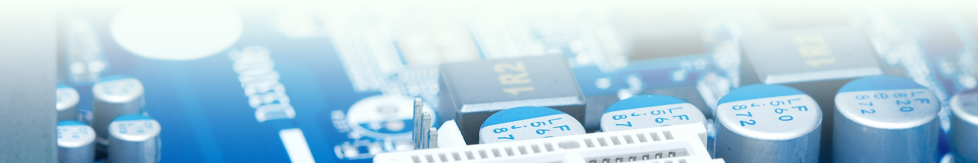
- Component Procurement: Electronic components such as resistors, capacitors, integrated circuits (ICs), diodes, transistors, connectors, and other passive and active components are sourced from suppliers. These components must meet the specifications outlined in the design documents.
- PCB Fabrication: The PCB is manufactured according to the design layout, which includes the placement of conductive traces, pads, and vias. The PCB may be single-sided, double-sided, or multi-layered, depending on the complexity of the circuit.
- Inspection and Cleaning: Both components and the PCB are inspected for defects and cleaned to remove any contaminants that could interfere with the assembly process or affect the reliability of the final product.
2. Component Placement
- Manual Placement: For low-volume production or prototypes, components may be placed manually using tweezers or other hand tools. This method is time-consuming but allows for greater flexibility in handling delicate or irregularly shaped components.
- Automated Placement (Pick-and-Place Machines): For high-volume production, automated pick-and-place machines are used to accurately and rapidly place components onto the PCB. These machines use vision systems to ensure precise placement and can handle a wide range of component sizes and shapes.
3. Soldering
- Wave Soldering: This method is typically used for through-hole components. The PCB is passed over a wave of molten solder, which wets the exposed leads and pads, creating a reliable electrical connection.
- Reflow Soldering: This method is used for surface-mount technology (SMT) components. A solder paste is applied to the PCB pads before component placement. The assembly is then heated in a reflow oven, causing the solder paste to melt and form solder joints between the components and the PCB.
- Selective Soldering: For assemblies with a mix of through-hole and SMT components, or for components that cannot withstand the high temperatures of reflow soldering, selective soldering may be used. This method involves applying solder only to specific areas of the PCB using a soldering iron or a laser.
4. Inspection
- Visual Inspection: After soldering, the assembly is visually inspected for any obvious defects, such as missing components, incorrect placement, or solder bridges (unintended connections between adjacent pads).
- Automated Optical Inspection (AOI): AOI systems use cameras and image processing software to automatically detect defects that may not be visible to the naked eye. These systems can quickly inspect large volumes of assemblies with high accuracy.
- X-Ray Inspection: For assemblies with hidden joints, such as ball grid arrays (BGAs), X-ray inspection may be used to verify the quality of the solder joints without damaging the assembly.
5. Testing
- In-Circuit Testing (ICT): ICT involves using a bed-of-nails fixture to make electrical contact with specific points on the PCB and test for open circuits, shorts, and component values. This test ensures that the assembly meets the electrical specifications outlined in the design.
- Functional Testing: Functional testing verifies that the assembled PCB performs its intended functions correctly. This may involve applying input signals and measuring output responses, or connecting the assembly to a larger system for integration testing.
- Environmental Testing: In some cases, the assembly may be subjected to environmental tests, such as temperature cycling, humidity testing, or vibration testing, to ensure its reliability under real-world conditions.
6. Final Assembly and Packaging
- Integration: The assembled PCB may be integrated into a larger system or product, such as a computer, smartphone, or industrial control unit. This step involves connecting the PCB to other components, such as displays, power supplies, and enclosures.
- Packaging: The final product is packaged for shipping and distribution. Packaging may include protective materials to prevent damage during transit, as well as labeling and documentation to provide information about the product and its usage.