
PCB Tests & Inspections
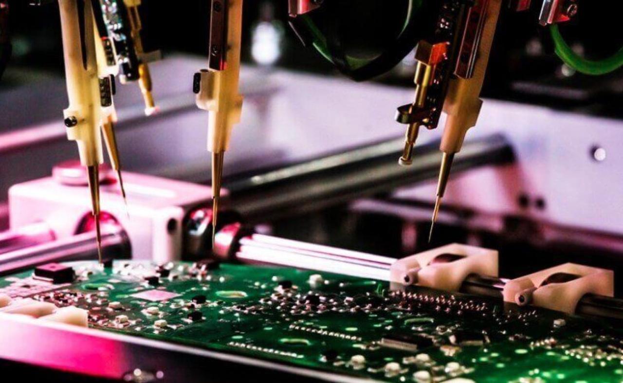
To make sure the highest quality printed circuit boards to our customers, we will implement a lot of testings and inspections during our PCB production processes or after PCBs are finished. Here are the main tests & inspections we have done.
- DFM(Design for Manufacturing) Check
- IQC (Incoming Quality inspection) for all materials
- Visual and mechanical inspection after every process
- Micro-section inspection
- Electrical Test for Open/short
- AOI (Automated Optical Inspection)
- TDR Impedance test
- Hi Potential Testing (Hi Pot PCB Testing).
- Any other tests customers required
- Visual Defects Inspection
- Solderability Test
- Thermal Test
- Tape Test (adhesion test)
- Peel Test (conductor peel strength)
- Ionic Contamination Test
- Inspect to IPC-A-600 Class 2 and IPC Class 3
- ICT(In-circuit Test) after PCB assembly
- FCT (FunctioDimensional Inspectionnal Test) after PCB assembly
IQC (Incoming Quality Inspection)
IQC (Incoming Quality Inspection) is a crucial process to ensure the quality of PCBs (Printed Circuit Boards). It is a complete inspection system aimed at finding any defects or inconsistencies in any of the material we used in PCB manufacturing. These material include CCL which is the most important one, copper, dry film, solder mask, silkscreen, and many more.
IQC should be undertaken with utmost attention to detail, as defective PCBs may lead to very high lost to both our customer and us. IQC can not only save on costs due to defect detection but also help maintain high levels of customer satisfaction by ensuring that products are built according to the highest standards. Therefore, IQC is essential for producing reliable and quality PCBs and should be noticed.
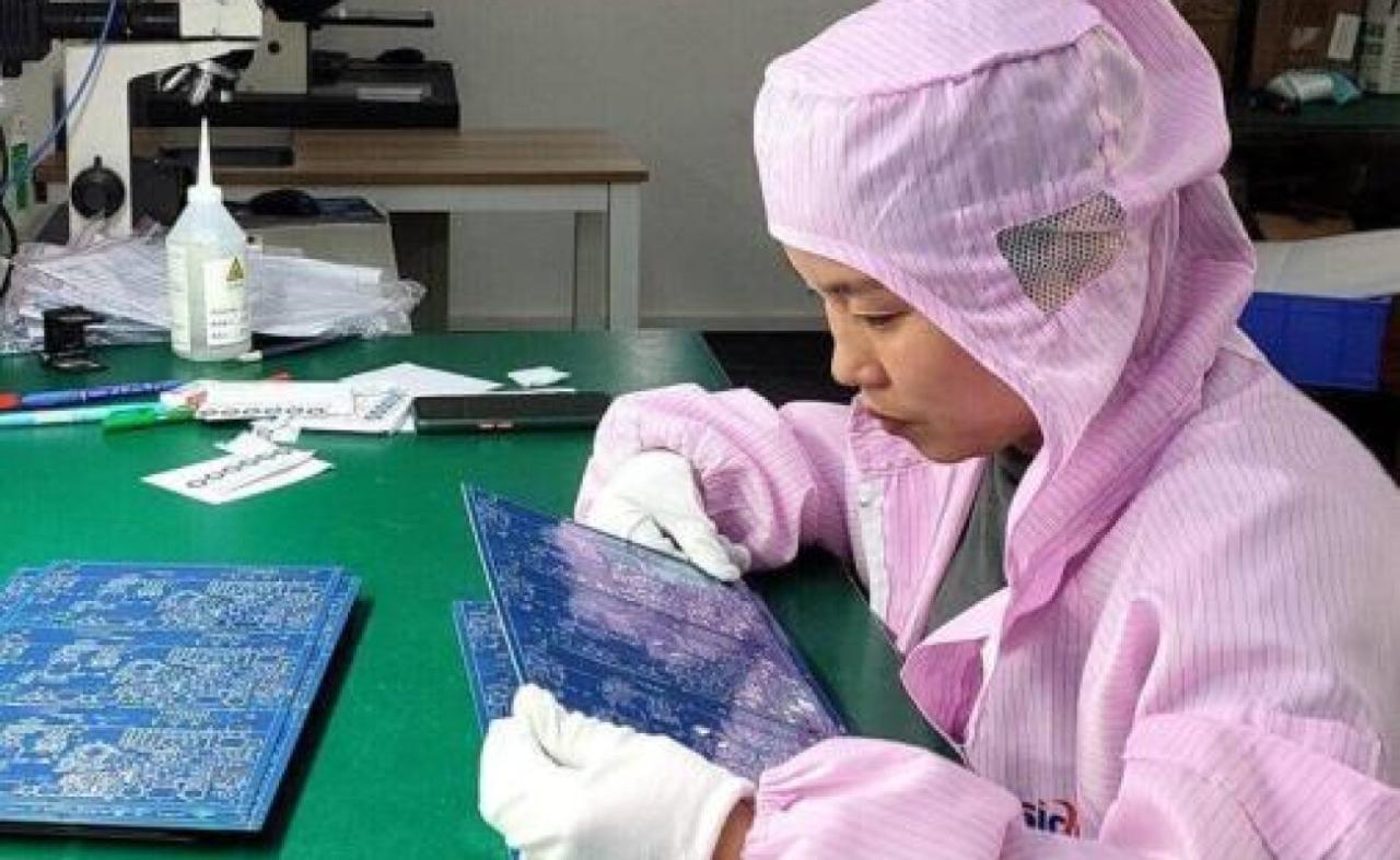
Manual Visual Inspection
Although AOI (Automated Optical Inspection) ,electrical test and other testing/inspections are used in our PCB manufacturing process, but manual visual inspection is still needed in a lot of places. Such as visual defects in base material, imperfection in solder mask, silkscreen etc. , since these minor defects cannot be defected by equipment. Manual Visual Inspection involves a meticulous visual examination of PCBs to detect any visual defects or flaws in the circuit boards before they are sent out for use.
This inspection gives us and our customers confidence that the product will perform according to IPC-A-600 Class 2 or 3 standards and customers’ standards. We ensure that our inspection process complies with the latest industry standards and best practices. So our inspection personnel have adequate training and experience and access to the required testing equipment.
Nowadays, advanced AVI (Automated Visual Inspection) machines are developed, but we think manual visual inspection is still needed.
AOI (Automated Optical Inspection)
AOI utilizes high-resolution cameras to capture images of PCBs at different angles, which are then compared to reference images to detect any defects or inconsistencies. Thus, manufacturers can quickly identify issues within their production lines without slowing production times or compromising quality control.
By leveraging AOI in PCB manufacturing processes, manufacturers can catch errors before they become costly problems down the line. It helps reduce waste and improves overall efficiency, as PCBs that would have passed inspection without AOI can be quickly identified and discarded. Manufacturers can keep up with their rigorous quality standards by using AOI technology in PCB production lines while ensuring a consistent end product.
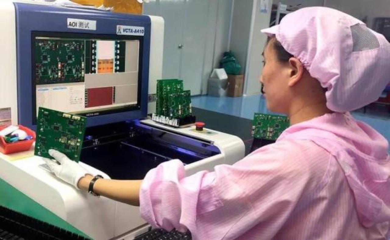
So, we think automated optical inspection (AOI) is an essential part of PCB manufacturing to ensure PCBs are free from defects and meet the highest quality standards.