The Complete Guide to : Process, Cost, and Quality Control
Welcome to the PCBA knowledge center at Brunnen. If you are sourcing a reliable partner for your electronics project or looking to optimize your current manufacturing supply chain, this guide is designed specifically for you.
For procurement professionals, engineers, and product managers, understanding the PCBA manufacturing process is essential for controlling product quality, managing costs, and ensuring timely delivery.
PCBA (Printed Circuit Board Assembly) manufacturing is far more than simply soldering components onto a circuit board. It is a complex engineering and supply chain process that integrates design verification, component sourcing, automated assembly, quality inspection, and functional testing.
This complete guide will walk you through the entire PCBA manufacturing ecosystem, helping you make smarter sourcing decisions and collaborate more effectively with your manufacturing partner.
Table of Contents
What is PCBA Manufacturing?
PCBA manufacturing refers to the process of assembling electronic components onto a Printed Circuit Board (PCB) to create a fully functional electronic circuit.
While a PCB is simply the bare circuit board, PCBA includes all mounted components such as:
- Integrated circuits (ICs)
- Resistors
- Capacitors
- Connectors
- Sensors
- Microcontrollers
The goal of PCBA manufacturing is to transform a circuit design into a fully operational electronic assembly ready to be integrated into a final product.
Modern PCBA production relies heavily on automation and precision machinery to assemble thousands of components accurately and efficiently.
For a deeper understanding, you can explore our related guide:
- PCB vs PCBA: What’s the Difference
PCBA Design Files and DFM Preparation
Before production begins, manufacturers require a complete set of engineering files.
The most critical files include:
Gerber Files
Gerber files define the physical layout of the PCB, including:
- Copper layers
- Lötmaske
- Silkscreen
- Drill holes
They serve as the blueprint for PCB fabrication.
Bill of Materials (BOM)
The BOM lists every component required for assembly, including:
- Manufacturer Part Number (MPN)
- Quantity
- Package type
- Electrical specifications
Accurate BOM documentation is essential for preventing supply chain delays.
Pick and Place File (CPL)
The Centroid or Pick-and-Place file determines the exact location and orientation of each component on the PCB.
Automated machines use this data to place components with high precision.
Design for Manufacturing (DFM)
Before assembly begins, responsible manufacturers perform a DFM review.
Design for Manufacturing analysis checks whether the PCB design is practical for production.
Typical DFM checks include:
- Pad spacing
- Component clearance
- Solder mask alignment
- Via placement
- Silkscreen overlap
Early DFM analysis helps prevent costly production errors.
Learn more in our detailed article:
- Design for Manufacturing (DFM) in PCBA
BOM and Component Sourcing Strategy
Component sourcing is the most critical supply chain element in PCBA manufacturing.
In many electronics projects, components account for 60–80% of the total production cost.
Procurement teams typically choose between two sourcing models.
Turnkey PCBA Manufacturing
In a turnkey model, the manufacturer manages the entire process:
- Beschaffung von Bauteilen
- PCB-Fertigung
- Montage
- Testing
- Delivery
This approach simplifies logistics and reduces sourcing complexity.
Turnkey PCBA is widely used by startups and OEM companies that want a single manufacturing partner.
Learn more:
- Turnkey PCBA Manufacturing Explained
Consigned PCBA Manufacturing
In the consigned model, the customer supplies some or all of the components.
This model is used when:
- Components are proprietary
- Pre-programmed chips are required
- Existing inventory must be used
However, consigned production requires careful supply chain management to avoid production delays.
Related article:
- Turnkey vs Consigned PCBA
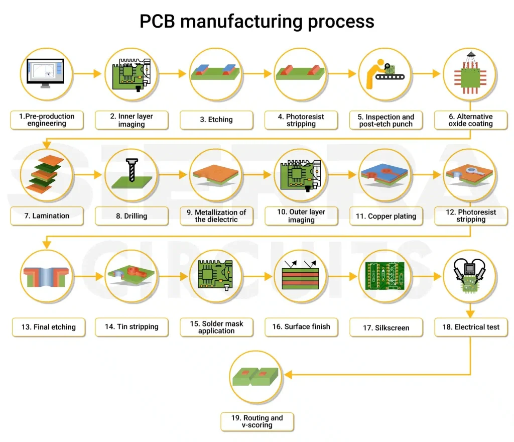
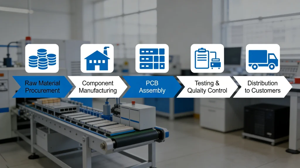
PCBA Manufacturing Process Step by Step
The PCBA manufacturing process involves several highly controlled stages.
PCB Fabrication
The PCB itself is manufactured according to the Gerber design files.
This process includes:
- Copper etching
- Layer lamination
- Drilling
- Surface finishing
Related guide:
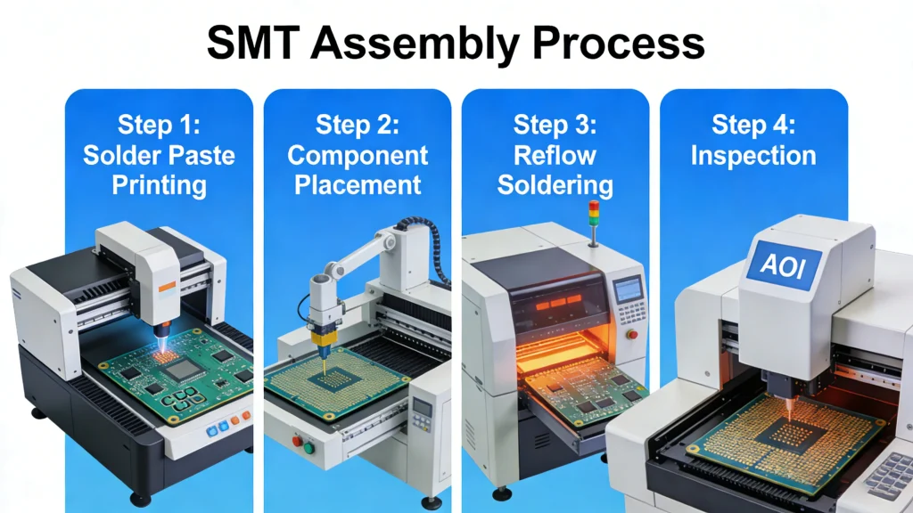
Solder Paste Printing
A stainless-steel stencil is used to apply solder paste onto PCB pads.
The paste contains tiny solder particles that will later form electrical connections.
SMT Component Placement
High-speed pick-and-place machines automatically place components onto the solder paste.
Modern machines can place tens of thousands of components per hour.
Reflow Soldering
The PCB passes through a reflow oven where controlled heat melts the solder paste.
When cooled, the solder solidifies to form strong electrical and mechanical connections.
Through-Hole Assembly
Certain components require Through-Hole Technology (THT) for stronger mechanical stability.
Examples include:
- Connectors
- Transformers
- Large capacitors
These components are typically soldered using wave soldering.
Inspection and Testing
After assembly, multiple inspections ensure product reliability.
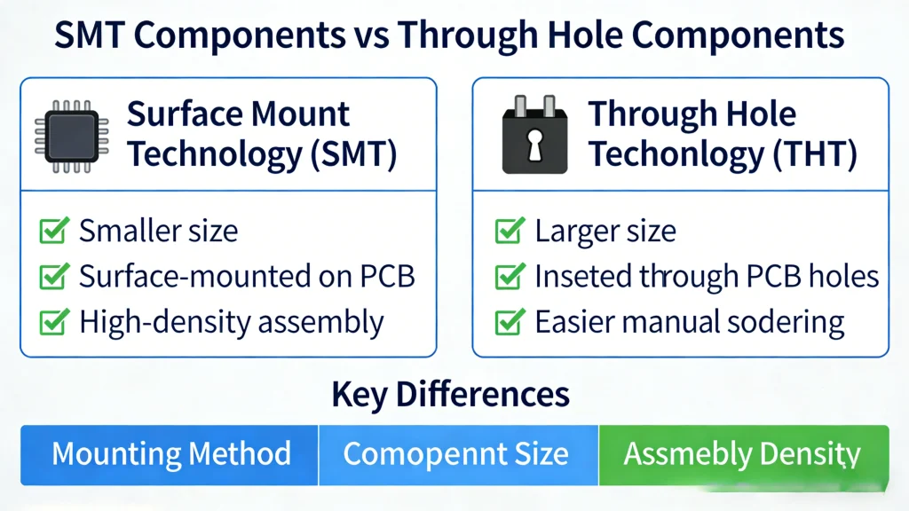
SMT vs THT Assembly Technologies
Two primary assembly technologies are used in PCBA manufacturing.
Surface Mount Technology (SMT)
SMT is the dominant assembly method for modern electronics.
Advantages include:
- High component density
- High automation
- Lower production cost
- Faster assembly
Most components in modern devices are SMT components.
Learn more:
- SMT Assembly Process
Through-Hole Technology (THT)
THT components have leads that pass through holes in the PCB.
This method provides stronger mechanical bonding.
THT is commonly used for:
- Power electronics
- Industrial equipment
- Mechanical connectors
Related article:
- SMT vs THT Assembly
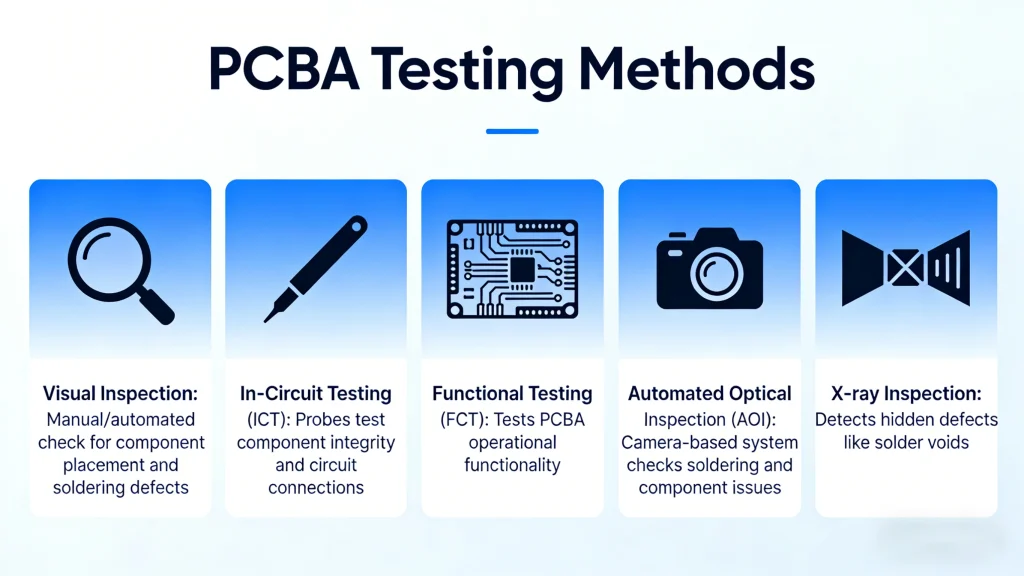
PCBA Testing and Quality Control
Quality control is essential in PCBA manufacturing.
Professional manufacturers integrate inspection throughout the entire production process.
Automated Optical Inspection (AOI)
AOI uses high-resolution cameras to detect assembly defects such as:
- Missing components
- Solder bridges
- Component misalignment
- Tombstoning
AOI is widely used for SMT quality inspection.
X-ray Inspection
X-ray inspection is required for components with hidden solder joints such as BGA packages.
It detects:
- Void formation
- Solder bridges
- Short circuits
Functional Circuit Testing (FCT)
Functional testing verifies that the completed PCBA performs its intended electronic functions.
This stage simulates the real operating environment of the product.
Learn more:
- PCBA Functional Testing Methods
Industry Standards in PCBA Manufacturing
High-quality PCBA production follows internationally recognized industry standards.
The most widely used standard is IPC-A-610, which defines the acceptability of electronic assemblies.
It categorizes products into three quality classes:
Class 1 – General electronics
Class 2 – Dedicated service electronics
Class 3 – High-reliability electronics
Industries such as medical devices, aerospace, and automotive electronics often require IPC Class 3 standards.
Choosing the Right PCBA Manufacturer
Selecting the right manufacturing partner is critical for project success.
Procurement professionals should evaluate suppliers based on several factors:
- Manufacturing capability
- Quality control systems
- Supply chain stability
- DFM support
- Testing capability
- Production capacity
Working with an experienced partner like Wells PCBA can significantly reduce risk and accelerate product development.
Conclusion
PCBA manufacturing is a complex integration of engineering, manufacturing technology, and supply chain management.
From design validation and component sourcing to automated assembly and rigorous testing, each stage plays a vital role in delivering a reliable electronic product.
By understanding the entire process, procurement professionals and product developers can make more informed decisions when selecting manufacturing partners.
At Brunnen, we help companies transform innovative electronic designs into reliable, high-quality products.
If you have an upcoming electronics project, our team is ready to support your manufacturing needs.
FAQ about PCBA Manufacturing
What is PCBA manufacturing?
PCBA manufacturing is the process of assembling electronic components onto a printed circuit board to create a functional electronic assembly.
What is the difference between PCB and PCBA?
A PCB is the bare circuit board, while PCBA refers to the board after electronic components are assembled and soldered.
How long does PCBA manufacturing take?
Typical PCBA lead time ranges from 7 to 20 days, depending on component availability and production volume.
What is turnkey PCBA?
Turnkey PCBA means the manufacturer manages the entire process, including component sourcing, assembly, testing, and delivery.