
DFM in PCB Assembly: The Complete Design for Manufacturability Guide
DFM in PCB assembly — Design for Manufacturability — is the discipline of creating circuit board designs that can be fabricated, assembled, inspected, and tested reliably, at yield, and at cost. It is not a final review step before you submit Gerbers. It is a design philosophy that begins at the schematic stage and continues through layout, panelization, and file preparation.
Done correctly, DFM converts theoretical circuit designs into physically manufacturable products with first-pass yield rates of 95–99%. Skipped or applied too late, it is the leading cause of board respins, production holds, tombstoning, solder bridging, and the kind of three-week delays that derail product launches.
This guide is written from the manufacturer’s side of the table. After reviewing thousands of design files at Wells Electronics — from simple two-layer consumer boards to 16-layer HDI designs for medical and automotive applications — the patterns in what causes production problems are consistent, specific, and largely preventable. Every rule in this guide corresponds to a real failure mode our engineers see in submitted designs.
What You’ll Learn in This Guide
- What DFM in PCB assembly actually means — and how it differs from DRC
- The 8 most critical DFM rule categories, with specific measurements
- The most common DFM violations seen from a manufacturer’s perspective
- How panelization, fiducial marks, and stencil aperture design affect assembly yield
- A complete DFM pre-submission checklist
- How Wells performs DFM review before any production begins
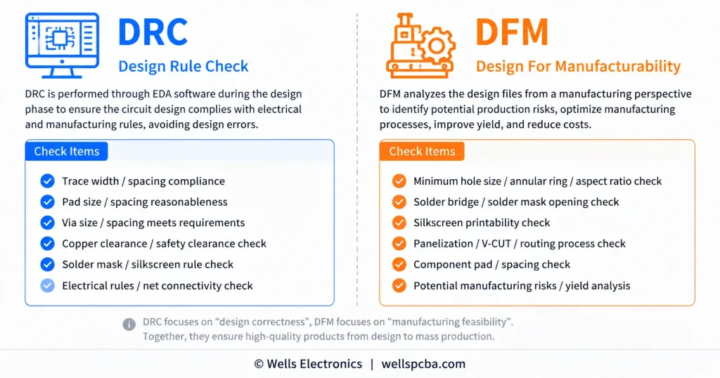
DFM vs. DRC: Why Your Design Rule Check Is Not Enough
DFM (Design for Manufacturability) and DRC (Design Rule Check) are different tools with different scopes. DRC validates a design against the rules programmed into your EDA software — it checks electrical connectivity, net violations, and the minimum feature sizes you have defined. DFM validates a design against the actual physical capabilities of the manufacturing process, equipment, and materials at a specific factory. A design can pass DRC completely and still fail catastrophically in production.
The gap between a passing DRC and a manufacturable design is where most first-time production problems live. Common examples of DRC-passing, DFM-failing conditions:
- Via-in-pad without fill specification: passes DRC (vias are allowed), causes solder wicking and weak joints in production
- Symmetric pad geometry on a 0402 resistor near a copper pour: passes DRC, causes tombstoning in reflow
- Component-to-edge clearance of 0.15mm: may pass your design rules, fails the manufacturer’s depaneling requirements
- Stencil aperture ratio below 0.66: not checked by any EDA DRC, causes inconsistent paste release and open solder joints
- Missing fiducial marks: DRC has no rule for this, pick-and-place machine cannot align to the board
The fundamental principle of DFM is that manufacturing constraints must be incorporated into the design, not applied as a filter afterwards. As IPC-7711/7721 — the IPC standard for rework, repair, and modification — documents extensively, the cost of correcting a design issue multiplies by approximately 10× at each stage from design → prototype → production → field deployment. (IPC International)
Category 1: Component Placement — The Foundation of Assembly Yield
Component placement is where the majority of DFM violations originate. Placement decisions made during floor planning determine whether reflow soldering produces consistent joints, whether automated inspection can reach every pad, and whether rework is possible without removing adjacent components.
Spacing Rules for SMT Components
The minimum clearances between components are not arbitrary — they reflect the physical space required for solder paste deposit, pick-and-place nozzle approach angles, AOI camera angles, and hot-air rework access.
| Clearance Type | Minimum Standard | Recommended |
|---|---|---|
| SMD to SMD (same height class) | 0.20 mm | 0.30 mm |
| SMD to through-hole component | 1.0 mm | 1.5 mm |
| SMD to board edge | 0.50 mm | 1.0 mm |
| BGA to any adjacent component | 1.0 mm | 2.0 mm |
| Tall component to any SMD (shadow exclusion) | 3× component height | 5× component height |
| Component to panelization score line | 5.0 mm | 7.0 mm |
The shadow exclusion zone for tall components deserves particular attention. During reflow soldering, tall components — connectors, electrolytic capacitors, transformers — create thermal shadows that reduce the heat reaching adjacent low-profile SMDs. A 0402 resistor placed within 1mm of a 15mm-tall capacitor will experience a different thermal profile than the rest of the board, which can produce cold joints or tombstoning specifically at that location.
Component Orientation Rules
Uniform component orientation is a critical and frequently overlooked DFM requirement. All passive components of the same value and package size should be oriented in the same direction on the board. There are two reasons:
- Reflow thermal balance: During reflow, pads heat at slightly different rates depending on their orientation relative to the oven conveyor direction. Consistent orientation allows the reflow profile to be optimized globally rather than per-component.
- Assembly efficiency: Placement programs for pick-and-place machines run faster when similar components share rotation values. Inconsistent orientations increase programming time and nozzle rotation wear.
The specific requirement per IPC-7351: all polarized components (diodes, tantalum capacitors, electrolytic capacitors) must have their polarity indicator in a consistent direction — either all anodes facing up, or all cathodes facing up — across a given board family.
Double-Sided Assembly Placement Strategy
For boards requiring SMT on both sides, placement on the second (bottom) side must account for the second reflow pass. During the second reflow cycle, the bottom-side components from the first pass are re-exposed to reflow temperatures while inverted. Heavy components — connectors, large BGAs, power modules — can fall off during the second reflow if their solder joint surface tension is insufficient to hold them against gravity.
Rule: Place heavy components (mass >30g or large BGA packages) exclusively on the primary (top) side. Place lightweight passives (0402, 0201, 0603) on the secondary side. If heavy components must be on both sides, the secondary-side heavy components require selective soldering, glue-dot fixturing, or manual placement after both reflows.
Category 2: Trace Routing and Copper Features
Minimum Trace Width and Spacing
Trace geometry directly affects fabrication yield. Traces narrower than the manufacturer’s process capability are at risk of etching open; traces spaced too close together risk etching bridges.
| Parameter | Standard Process | Advanced Process |
|---|---|---|
| Minimum trace width | 5 mil (0.127mm) | 3 mil (0.076mm) |
| Minimum trace spacing | 5 mil (0.127mm) | 3 mil (0.076mm) |
| Recommended power trace width (1A) | 10 mil (0.254mm) | — |
| Recommended power trace width (3A) | 20 mil (0.508mm) | — |
| Trace-to-board-edge clearance | 10 mil (0.254mm) | — |
| Trace-to-copper-pour clearance | 8 mil (0.203mm) | — |
Always request and program the specific manufacturer’s DFM capability document into your EDA design rules before layout begins. At Wells Electronics, our standard process supports 4/4 mil trace/space; our advanced process supports 3/3 mil. Designing to 3/3 mil on a factory with a 4/4 mil process creates fabrication failures that are invisible in your DRC. For more on how these parameters integrate into the production workflow, see the PCBA manufacturing process guide.
Avoiding Acid Traps
Acute angles (less than 90°) in trace routing create “acid traps” — locations where etchant chemistry pools during the chemical etching process, over-etching the copper and creating potential open circuits. This is a classic DFM violation that passes every DRC but causes fabrication failures.
Rule: Route traces at 45° or 90° angles only. Never route at acute angles. If your autorouter produces acute-angle jogs, clean them manually before file submission.
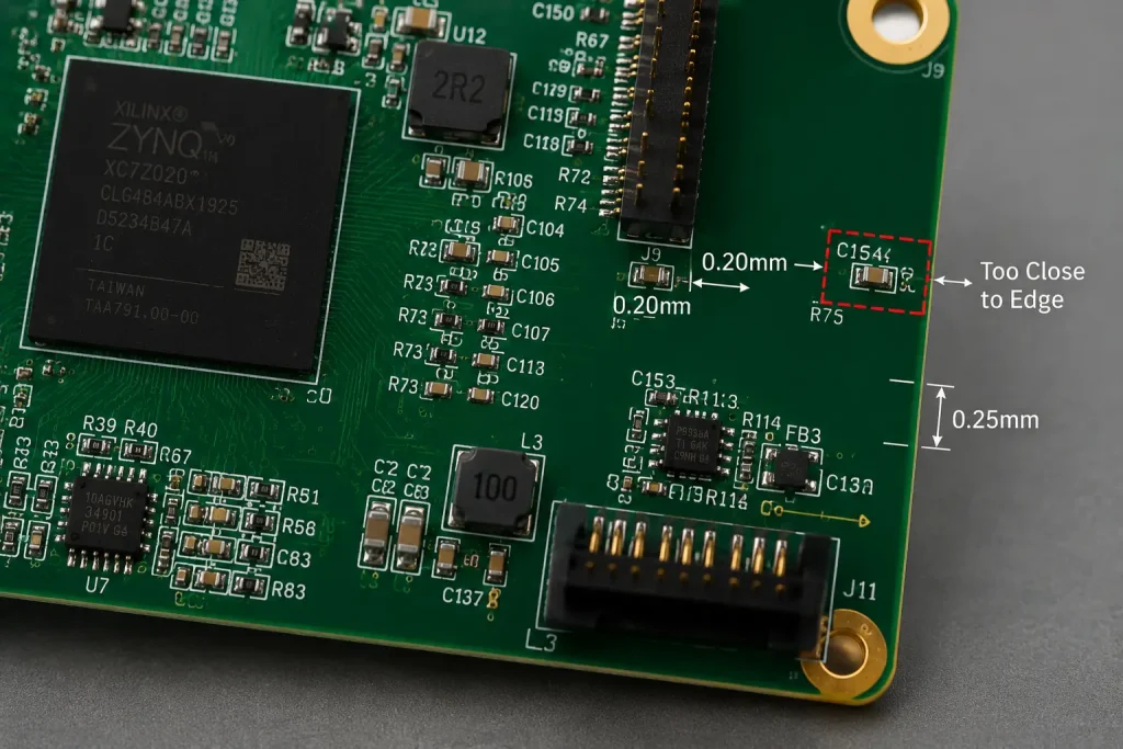
Copper-to-Board-Edge Clearance
Copper features placed too close to the board edge are at risk of physical damage during routing (V-score or mechanical routing) and from handling during assembly. Exposed copper at the board edge also presents a corrosion risk in the field.
Rule: Maintain minimum 0.25mm (10 mil) clearance between any copper feature and the board edge. For high-voltage designs, increase to 0.5mm. For designs with edge-launch connectors, clarify edge clearance requirements with the manufacturer before layout.
Category 3: Via Design — The Most Common Source of Solder Defects
Vias are the single most DFM-critical feature in a multilayer PCB design. Incorrect via placement and specification produce several of the most frustrating assembly defects: solder wicking through via barrels, voids under BGAs, cold joints from thermal drain, and solder balls scattered across the board.
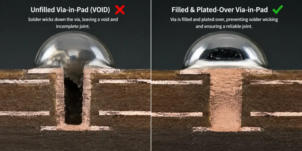
Via-in-Pad: When It’s Acceptable and How to Specify It Correctly
Via-in-pad — placing a through-hole or microvia directly within an SMT pad — is common in HDI designs, particularly under BGA thermal pads and in fine-pitch routing escape. It creates a real manufacturing challenge: uncapped vias in pads act as solder drains during reflow, wicking solder away from the joint and creating voids, insufficient solder, or complete opens.
The DFM rule: Via-in-pad is acceptable only when specified and fabricated correctly. The via must be:
- Filled: Filled with non-conductive or conductive epoxy to prevent solder wicking
- Planarized: Ground flat after filling to ensure the pad surface is level
- Plated over (capped): Copper-plated over the filled via to create a solid, solderable pad surface
This specification must be explicitly stated in your fabrication notes. “Via-in-pad, filled and capped per IPC-4761 Type VII” is the correct notation. Without this note, the manufacturer may leave the via open, and your assembly will have voids.
For designs not requiring via-in-pad, the minimum distance from the edge of an SMT pad to the edge of the nearest via should be 0.1mm (4 mil) with a solder mask dam between them. If a via must be within 0.1mm of a pad, it must be tented (solder mask covered) to prevent solder wicking.
Via Aspect Ratio
The aspect ratio of a through-hole via (depth ÷ diameter) determines whether it can be reliably plated. As aspect ratio increases, electroplating solution has greater difficulty reaching the center of the barrel, resulting in thin or non-uniform copper plating.
Rule: Maintain via aspect ratio ≤8:1 for standard fabrication. For aspect ratios >10:1, consult the manufacturer — specialized plating processes and additional cost are required. Example: a 1.6mm thick board with a 0.2mm drill diameter has an aspect ratio of 8:1 — the borderline limit for standard processing.
Annular Ring Requirements
The annular ring is the copper pad material surrounding a drilled hole. Insufficient annular ring width risks “breakout” — the drill hole exits the pad — creating an open circuit or a mechanically weak connection.
Per IPC-6012 Class 2 (standard commercial): minimum annular ring 100µm (4 mil) for outer layers, 50µm (2 mil) for inner layers. Per IPC-6012 Class 3 (high-reliability): minimum annular ring 125µm (5 mil) outer, 75µm (3 mil) inner.
These are post-fabrication measurements. To achieve them, your designed annular ring must be wider to account for drill position tolerance (typically ±75µm for mechanical drilling, ±25µm for laser drilling).
Category 4: Solder Mask Design
Solder Mask Expansion (SMD Pad Openings)
The solder mask opening must be sized correctly relative to the copper pad. Too small and it covers the solderable surface; too large and it leaves exposed copper between adjacent pads, inviting solder bridging.
Standard rule: Solder mask expansion of +0.05mm (2 mil) per side beyond the copper pad edge. For fine-pitch components (pitch ≤0.5mm), use 0 expansion — the mask opening matches the pad exactly — to preserve the solder mask dam between pads.
Solder Mask Dams Between Fine-Pitch Pads
A solder mask dam is the thin strip of mask material between adjacent pads on a fine-pitch component. Its purpose is to prevent solder from flowing between pads during reflow and creating a bridge.
Critical rule: Minimum solder mask dam width of 0.1mm (4 mil) for standard processes. For QFN, fine-pitch QFP, and 0.5mm-pitch BGA, verify with the manufacturer that their mask resolution can hold 0.1mm dams at the specified pitch. If the dam width required is below the manufacturer’s capability, the design must use solder mask defined (SMD) pads — where the mask opening is smaller than the copper pad — rather than non-solder-mask-defined (NSMD) pads.
Silkscreen Clearances
Silkscreen (legend) text and component outlines must not overlap solder mask openings (pad areas). Silkscreen ink deposited on a pad contaminates the solderable surface and causes poor solder wetting.
Rules:
- Minimum clearance from silkscreen to pad edge: 0.15mm (6 mil)
- Minimum silkscreen line width: 0.1mm (4 mil) for legibility after assembly
- Reference designators must remain visible after component placement — do not place designators under components
Category 5: Thermal Relief and Heat Management in Layout
Thermal management in PCB layout is a DFM concern before it becomes a thermal engineering concern. Poor thermal design at the layout stage causes assembly defects; poor thermal engineering causes field failures. Both are preventable at the DFM stage.
Thermal Relief Connections to Copper Planes
When a through-hole pad or SMT pad connects directly to a large copper plane (power or ground pour), the plane acts as a heat sink during soldering. The solder joint may fail to reach liquidus temperature while the surrounding copper absorbs heat — producing a cold joint or, for THT components, incomplete barrel fill.
Rule: All through-hole pads connected to internal copper planes must use thermal relief connections — spoke connections that limit heat transfer to the plane. Standard thermal relief uses 4 spokes at 45°/135° angles, 0.25mm (10 mil) spoke width, 0.25mm (10 mil) air gap.
For SMT pads connected to planes, use thermal relief when the component is a passive (resistor, capacitor) or a package with thermal mass less than the surrounding pour. For power components (MOSFETs, linear regulators, power diodes) that require maximum thermal conductivity to the plane, solid connection is appropriate — but this must be an intentional design decision, not a default.
Thermal Vias Under Power Components
Power components that dissipate significant heat require a thermal pathway from the component’s exposed pad to inner or bottom-side copper planes. Thermal vias — small vias (0.3mm drill) in a grid pattern under the component pad — provide this pathway.
DFM specification for thermal vias:
- Drill diameter: 0.3mm (12 mil)
- Via fill: Required if vias are in-pad (to prevent solder wicking) — specify “filled and capped” per IPC-4761
- Grid pattern: 0.6–0.8mm pitch for standard thermal via arrays
- Minimum 4 vias, recommended 9+ vias for packages >3mm × 3mm
This is one of the most common omissions in designs from teams that are strong on electrical engineering but less experienced with thermal management. The PCB soldering defects guide covers the cold joint and delamination failures that result when thermal management is insufficient.
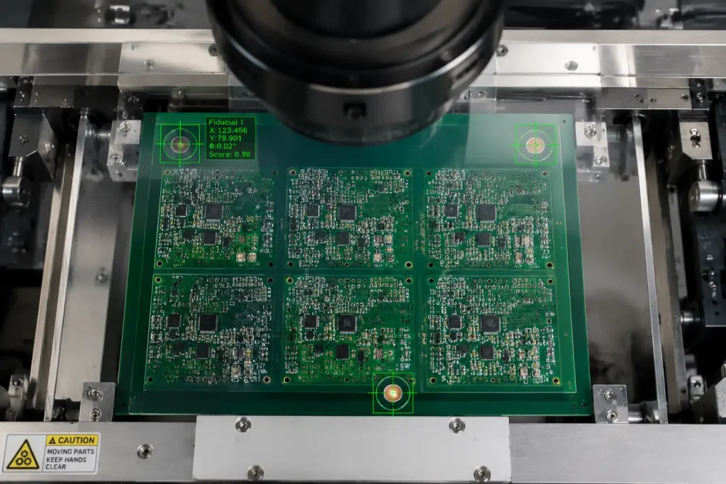
Category 6: Fiducial Marks and Tooling Features
Fiducial marks are small, bare copper circles on the PCB surface that serve as optical reference points for the pick-and-place machine’s vision system. They are not electrical features. They have no net connection. But without them, automated assembly cannot begin — or more precisely, it begins with a systematic alignment error that produces the same placement offset on every component.
Fiducial Mark Specifications
| Parameter | Requirement |
|---|---|
| Mark geometry | Solid copper circle (no solder mask opening required, but recommended) |
| Mark diameter | 1.0–2.0mm (1.0mm most common) |
| Solder mask opening diameter | 3× fiducial diameter (3.0mm for a 1.0mm mark) |
| Copper-free keepout zone | 3mm radius around the mark (no copper features, no traces) |
| Minimum quantity per board/panel | 3 global fiducials |
| Placement pattern | Non-symmetrical triangle (prevents 180° rotation errors by the vision system) |
| Placement position | Near panel/board corners, minimum 5mm from board edge |
Global vs. Local Fiducials
Global fiducials are placed at the corners of the panel or board and allow the machine to correct for X, Y, and rotational offset of the entire board relative to the machine coordinate system.
Local fiducials are placed adjacent to fine-pitch components — specifically, BGAs with pitch ≤0.8mm, fine-pitch QFPs with pitch ≤0.5mm, and fine-pitch QFN packages. Local fiducials provide a secondary alignment reference that corrects for local stretch/shrink of the laminate near the component, achieving placement accuracy at the individual component level rather than the board level.
Requirement: Any design containing BGA packages, fine-pitch QFP (pitch ≤0.5mm), or 0.4mm-pitch QFN must include local fiducials within 15mm of each such component.
Tooling Holes
Tooling holes are non-plated through-holes used to mechanically fixture the PCB in assembly equipment and test fixtures. They are distinct from fiducial marks (which are optical) and from mounting holes (which are part of the product’s mechanical assembly).
Rule: Minimum 2 tooling holes per board/panel, placed at diagonally opposite corners, diameter 3.2mm (1/8 inch), toleranced to ±0.05mm. Tooling holes must be mechanically isolated — no copper keepout or circuit features within 0.5mm.
Category 7: Panelization and Depanelization
Single PCBs are rarely assembled individually on a production line. Most boards are fabricated and assembled in panels — arrays of multiple boards on a single sheet — which then pass through the entire SMT line as a unit. The panel is depanelized (separated into individual boards) after assembly, either before or after testing.
Panel Design Requirements
A well-designed panel satisfies several constraints simultaneously: it maximizes board density to reduce per-board fabrication cost, maintains sufficient mechanical rigidity for conveyor transport, provides the tooling features required for automated assembly, and allows clean depanelization without mechanical stress on solder joints or components.
Step 1 — Define panel size: Most SMT lines accommodate panels up to 460mm × 610mm. Panels smaller than 50mm × 50mm cannot be fixtured reliably. Confirm your manufacturer’s panel size range before designing the array.
Step 2 — Add tooling strips: If individual boards are too small to accommodate fiducial marks and tooling holes at their corners, add tooling strips (typically 5mm wide) along two parallel edges of the panel. These strips carry the fiducials and tooling holes for the entire panel.
Step 3 — Choose the separation method: V-score (V-groove) for rectangular boards without components within 5mm of the board edge; tab routing (breakaway tabs) for irregular shapes or boards with edge-mounted components. V-score is faster and lower cost; tab routing preserves edge-mounted components but requires break-out force after assembly.
Step 4 — Set component-to-edge clearance: Components within 5mm of a V-score line will experience mechanical stress during depanelization. This stress can crack solder joints, particularly on ceramic capacitors (which are brittle). Maintain minimum 5mm clearance from any component to the nearest V-score or routing line.
Step 5 — Specify on the fab drawing: Panel configuration, separation method, tooling strip dimensions, fiducial positions, and individual board location must all be explicitly defined on the fabrication drawing. Do not leave panelization to the manufacturer’s judgment — their default panel configuration may not match your assembly or test fixture.
Category 8: Stencil Aperture Design and Solder Paste Management
The SMT stencil — a laser-cut stainless steel sheet through which solder paste is printed onto the board — is the first manufacturing tool in the assembly process. Its design determines paste volume on every pad. Get it right and first-pass yield begins at 98%+. Get it wrong and every board in the batch has the same solder volume defect.
The Area Ratio Rule
The area ratio is the ratio of the stencil aperture opening area to the aperture wall area (perimeter × stencil thickness). It determines whether solder paste will release cleanly from the aperture onto the pad, or will stick to the aperture walls and produce an insufficient deposit.
Formula: Area Ratio = (Aperture Length × Aperture Width) ÷ (2 × Stencil Thickness × (Aperture Length + Aperture Width))
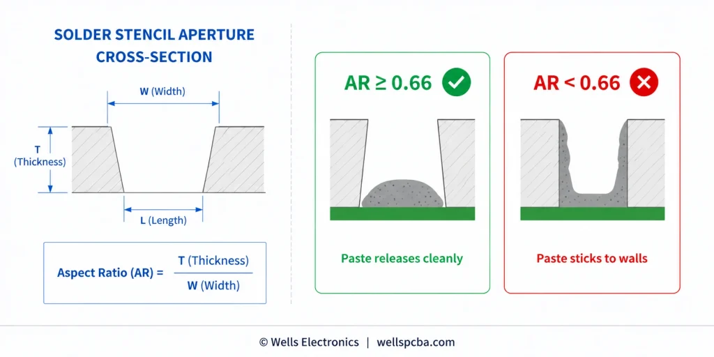
Rule: Area ratio must be ≥0.66 for consistent paste release with standard solder paste. Below 0.66, paste sticking increases, volume inconsistency increases, and open solder joints become likely.
Practical implication: for a standard 0.12mm (5 mil) stencil thickness, the minimum aperture dimension is approximately 0.28mm × 0.28mm. For smaller pads (01005 components, 0.3mm-pitch BGA), a thinner stencil (0.08mm or 0.10mm) is required to maintain area ratio compliance.
Aperture Reduction for Fine-Pitch Components
For fine-pitch QFN, QFP, and 0.5mm-pitch BGA, the aperture is typically reduced to 80–90% of the pad size to limit paste volume and prevent bridging. This aperture reduction must be specified in the stencil design file, not assumed by the manufacturer.
Common DFM error: Designers submit paste layer files with apertures sized 1:1 to the copper pads, without applying fine-pitch reduction. The manufacturer cuts the stencil exactly as specified. The result is excess paste on fine-pitch pads, bridging during reflow, and 100% rework on every board.
Solder Paste Inspection (SPI) — Why Your Stencil Design Affects Yield Even After Printing
Modern professional PCBA lines use inline 3D SPI (Solder Paste Inspection) immediately after paste printing to measure paste volume, height, and alignment on every pad before component placement. A well-designed stencil produces paste deposits within ±15% of nominal volume — acceptable for reliable soldering. A poorly designed stencil produces paste deposits outside ±25% — unacceptable, requiring the board to be cleaned and re-printed, adding cycle time and increasing the risk of paste contamination.
For more on how SPI and subsequent inspection stages form the quality gate in professional assembly, see What Is PCBA Manufacturing?
The DFM-Critical File Package: What to Submit and How
A complete, DFM-ready file submission eliminates 80% of the back-and-forth that delays production starts. The following file set is required for professional PCBA manufacturing:
Step 1 — Gerber files (RS-274X or ODB++format)
- All copper layers (top, bottom, inner layers)
- Solder mask layers (top and bottom)
- Silkscreen layers (top and bottom)
- Paste mask layers (top and bottom) — critical for SMT stencil fabrication, often omitted by inexperienced designers
- Board outline layer (mechanical/keepout layer)
- NC drill file (Excellon format with separate drill list)
Step 2 — Bill of Materials (BOM)
- Part number, manufacturer P/N, approved alternate P/N(s), quantity, reference designators
- No “TBD” or “any equivalent” entries — every line must be resolved before production
- For high-reliability builds: include distributor source requirements (authorized distributor only)
Step 3 — Pick-and-Place (Centroid) file
- Reference designator, X coordinate, Y coordinate, rotation, side (top/bottom) for every SMT component
- Coordinates measured from a consistent origin point (typically board lower-left corner)
- Rotation values in degrees, 0° = standard package orientation
Step 4 — Assembly Drawing (IPC-D-325 or PDF)
- Board outline with dimensions
- Component placement view (top and bottom)
- Special assembly notes: polarity requirements, keep-out zones, conformal coating areas, specific torque values for hardware
Step 5 — Special notes in fabrication document
- IPC performance class (Class 2 or Class 3)
- Controlled impedance requirements with target values and tolerance
- Via fill specifications (via-in-pad, tenting requirements)
- Surface finish specification
- Panelization requirements (if not pre-panelized by the designer)
For a full overview of how these files integrate into the turnkey manufacturing workflow, see the Turnkey PCBA Ultimate Guide.
The 15 Most Common DFM Violations — From a Manufacturer’s Perspective
After reviewing tens of thousands of design submissions, these are the violations that cause the most production holds, board respins, and assembly failures:
- Via-in-pad without fill specification — causes solder wicking, voids under BGA thermal pads. Fix: specify “filled and capped, IPC-4761 Type VII.”
- Missing paste layer files — stencil cannot be fabricated. Fix: generate and include .GTP/.GBP files.
- Missing or insufficient fiducial marks — automated placement cannot begin. Fix: add ≥3 global fiducials in non-symmetrical triangle.
- BOM with unresolved “TBD” or “any equivalent” entries — procurement hold before production starts. Fix: resolve every BOM line before submission.
- Component spacing violations near board edge — mechanical damage during depanelization. Fix: 5mm minimum from V-score, 1mm minimum from routed edge.
- Tombstoning risk: asymmetric pad geometry on passives connected to copper pours — uneven reflow heating causes one end to lift. Fix: add thermal relief spokes; ensure symmetric copper connections.
- Solder mask bridge violation on fine-pitch pads — mask dam below 0.1mm causes bridging. Fix: verify mask dam width against manufacturer’s resolution capability.
- Trace acid traps (acute angles) — over-etching creates opens. Fix: use 45°/90° routing only.
- Stencil aperture area ratio <0.66 — inconsistent paste release, opens. Fix: reduce aperture length/width ratio or decrease stencil thickness.
- Missing local fiducials near BGA packages — systematic placement offset on fine-pitch balls. Fix: add local fiducials within 15mm of each BGA.
- Silkscreen overlapping pad openings — silk ink contaminates solderable surface. Fix: maintain 0.15mm clearance from silk to pad edge.
- Via aspect ratio >8:1 — thin or discontinuous barrel plating. Fix: increase via diameter or use laser-drilled microvias for HDI designs.
- No thermal relief on THT pads connected to inner planes — cold joints, incomplete barrel fill. Fix: add thermal relief spokes on all plane-connected THT pads.
- Centroid file with incorrect rotation values — components placed at wrong orientation. Fix: verify centroid rotation against library footprint standard orientation before submission.
- Heavy components on secondary side without adhesive specification — components fall during second reflow. Fix: relocate to primary side, or specify component adhesive and cure parameters.
How Wells Electronics Performs DFM Review
At Wells Electronics, every order — from a 5-board prototype to a 5,000-unit production run — goes through a human DFM review before any production activity begins. This is not an automated Gerber viewer check. It is a review by a process engineer who evaluates the design against Wells’ manufacturing capabilities and the specific requirements of your application.
The DFM review at Wells covers:
- Pad geometry and stencil compatibility: aperture area ratio, fine-pitch reduction requirements, via-in-pad treatment
- Component placement: spacing violations, shadow zones, second-side heavy component risk, fiducial adequacy
- Trace and via design: trace width/spacing against our process capability, via aspect ratio, acid trap detection
- Thermal management: thermal relief presence on plane-connected pads, thermal via specification under power components
- File completeness: paste layer presence, centroid file accuracy, BOM resolution, special note clarity
- Panelization: if not pre-panelized, Wells recommends panel configuration based on board size and our line specifications
DFM review is completed within 24 hours of file receipt and delivered as an annotated report with specific findings, measurements, and recommended corrections — not a pass/fail verdict. Customers with complex designs or tight timelines are assigned a dedicated process engineer for pre-submission consultation.
This review is a standard part of our service — not an upsell, not a fee, and not a gate that adds time to the schedule when the design is clean. It exists because catching a via-in-pad specification error before production starts takes 20 minutes. Catching it after assembly of 500 boards takes much longer.
To understand how DFM review integrates into the full production workflow, see the PCBA Manufacturing Guide and SMT vs. THT Assembly for the specific assembly stage considerations that DFM addresses.
For high-volume production programs, DFM review generates the process control baseline data — stencil aperture parameters, reflow profile selection, AOI recipe configuration — that carries through the production lifecycle. See High-Volume PCB Assembly Services for how this translates to volume production yield management.
Submit your design files for a free DFM review →
The DFM Pre-Submission Checklist
Use this checklist before submitting any PCB design for manufacturing. Print it, keep it in your EDA tools folder, or bookmark this page.
File Completeness
- All Gerber layers present including paste mask (.GTP/.GBP)
- NC drill file in Excellon format with drill list
- Pick-and-Place (centroid) file with reference designators, X/Y, rotation, side
- BOM with all lines fully resolved — no TBD, no “any equivalent”
- Assembly drawing with special notes
- IPC class specified in fabrication notes
Component Placement
- Minimum 0.20mm spacing between all SMT components
- Minimum 5mm from any component to V-score depanelization line
- Minimum 3 global fiducial marks in non-symmetrical triangle
- Local fiducials added within 15mm of all BGA and fine-pitch QFP/QFN
- Heavy components confirmed on primary side, or adhesive specified for secondary side
- All polarized components oriented consistently
Via and Pad Design
- Via-in-pad: all instances specified as filled and capped (IPC-4761 Type VII)
- Via aspect ratio ≤8:1 for all through-hole vias
- Annular ring ≥100µm (Class 2) or ≥125µm (Class 3) outer layer
- Via-to-pad clearance ≥0.1mm, or vias tented where closer
Trace Routing
- Minimum trace width/spacing confirmed against manufacturer capability
- No acute angles (acid traps) in trace routing
- Copper-to-board-edge clearance ≥0.25mm
Solder Mask
- Solder mask expansion +0.05mm per side (0 for fine-pitch ≤0.5mm pitch)
- Solder mask dams ≥0.10mm between fine-pitch pads
- Silkscreen clearance ≥0.15mm from all pad openings
Thermal
- Thermal relief on all THT pads connected to inner copper planes
- Thermal relief on SMT passive pads connected to pours
- Thermal via array specified under all power components with exposed thermal pads
Stencil
- Stencil aperture area ratio ≥0.66 for all pads
- Aperture reduction (80–90%) applied to fine-pitch pads ≤0.5mm pitch
- Stencil thickness specified in fabrication notes
FAQ
DFM stands for Design for Manufacturability. In PCB assembly, it refers to designing a circuit board so that it can be reliably fabricated, assembled by automated SMT equipment, inspected, and tested without requiring rework or redesign. DFM considers real-world process constraints — equipment capabilities, material behaviors, solder chemistry, and thermal dynamics — rather than just electrical design rules. A PCB design that passes its EDA design rule check (DRC) can still fail DFM if it violates manufacturing process requirements that DRC does not check.
DFM (Design for Manufacturability) addresses the fabrication and assembly process — trace widths, via specifications, solder mask clearances, stencil aperture design. DFA (Design for Assembly) addresses how components are arranged for efficient automated placement — floor planning, component orientation consistency, fiducial mark placement, and testability features. In practice, the terms are used interchangeably by many manufacturers. Both are evaluated in a professional pre-production review. (Wikipedia: Design for manufacturability)
DFM review should inform the design from the schematic stage, not be applied as a final check on finished Gerbers. The most impactful DFM decisions — layer stack-up, via strategy, component placement floor plan, panelization approach — must be made before layout begins. That said, a formal DFM review of completed Gerber files before production is essential and catches issues that accumulate during layout. The earlier in the design process that DFM constraints are applied, the lower the cost of any resulting changes.
The most costly DFM mistakes are those that are not detected until assembly is complete. Via-in-pad without fill specification produces solder voids under BGA packages that require X-ray inspection and rework of every affected joint. Missing fiducial marks can cause systematic placement offsets discovered only during first-article inspection after a full panel has been assembled. Heavy components on the secondary side without adhesive specifications can fall during reflow, requiring manual replacement of every affected component. These failures are entirely preventable with pre-production DFM review.
No. A manufacturer’s DFM review is a manufacturing capability check — it verifies that the design’s features (trace widths, via specifications, pad geometries) are within the factory’s process window. It is not a design review that checks signal integrity, power delivery, or functional correctness. The designer is responsible for ensuring the design works electrically; the manufacturer’s DFM review ensures it can be built. The two are complementary, not substitutes.
At Wells Electronics, DFM review is completed within 24 hours of receiving a complete file package (Gerbers, BOM, centroid file, and assembly drawing). Complex designs — multilayer HDI boards with multiple BGA packages, high-density fine-pitch arrays, boards requiring controlled impedance — may require up to 48 hours for a thorough review. DFM review is included at no charge with every quotation request.